Suppression of leakage current in image acquisition

a leakage current and image acquisition technology, applied in the direction of coupling device connection, radiation control device, instruments, etc., can solve the problems of leakage current flowing into the tfts, deteriorating image acquisition accuracy, and lowering light sensitivity

Active Publication Date: 2007-09-04
JAPAN DISPLAY CENTRAL CO LTD
View PDF12 Cites 6 Cited by
  • Summary
  • Abstract
  • Description
  • Claims
  • Application Information

AI Technical Summary

Benefits of technology

[0012]According to this invention, the defect density in the I layer of the photoelectric conversion element is made higher than the defect density in the channel portion of the switching element. Consequently, while suppressing the leakage current of the switching element, the sensitivity of the photoelectric conversion element to light can be improved.
[0014]According to this invention, the hydrogenation of the polysilicon layer is performed so as to set a defect density in the region for forming the photoelectric conversion element to be higher than a defect density in the region for forming the switching element. Thus it can be made possible to manufacture the display device in which the leakage current of the switching element can be suppressed, and the sensitivity of the photoelectric conversion element to light can be improved.
[0016]According to this invention, the gate electrode is provided above the i region of the pin-type optical sensor diode with an insulating film interposed therebetween, thus the threshold of the bias voltage when the current starts to flow into the optical sensor diode can be controlled by the gate voltage. Consequently, the leakage current can be prevented from flowing into the optical sensor diode to which no bias voltage higher than the gate voltage is applied even in the state where light is being irradiated.

Problems solved by technology

However, even if active layers of various TFTs (thin film transistors) formed on the array substrate are formed of polysilicon, when a number of dangling bonds exist in the active layers, there is a problem of a leakage current flowing into the TFTs.
However, in the case of the above-described contact-type area sensor, there is a problem in that, when the dangling bonds in the active layers are terminated, sensitivity to light is lowered.
Moreover, in an optical sensor diode used in a conventional image acquisition circuit, even if a reverse bias voltage is 0V, a weak leakage current is generated when light is irradiated, thus causing the accuracy of image acquisition deteriorate.

Method used


Image

  • Suppression of leakage current in image acquisition
  • Suppression of leakage current in image acquisition
  • Suppression of leakage current in image acquisition

Examples


first embodiment

1. First Embodiment

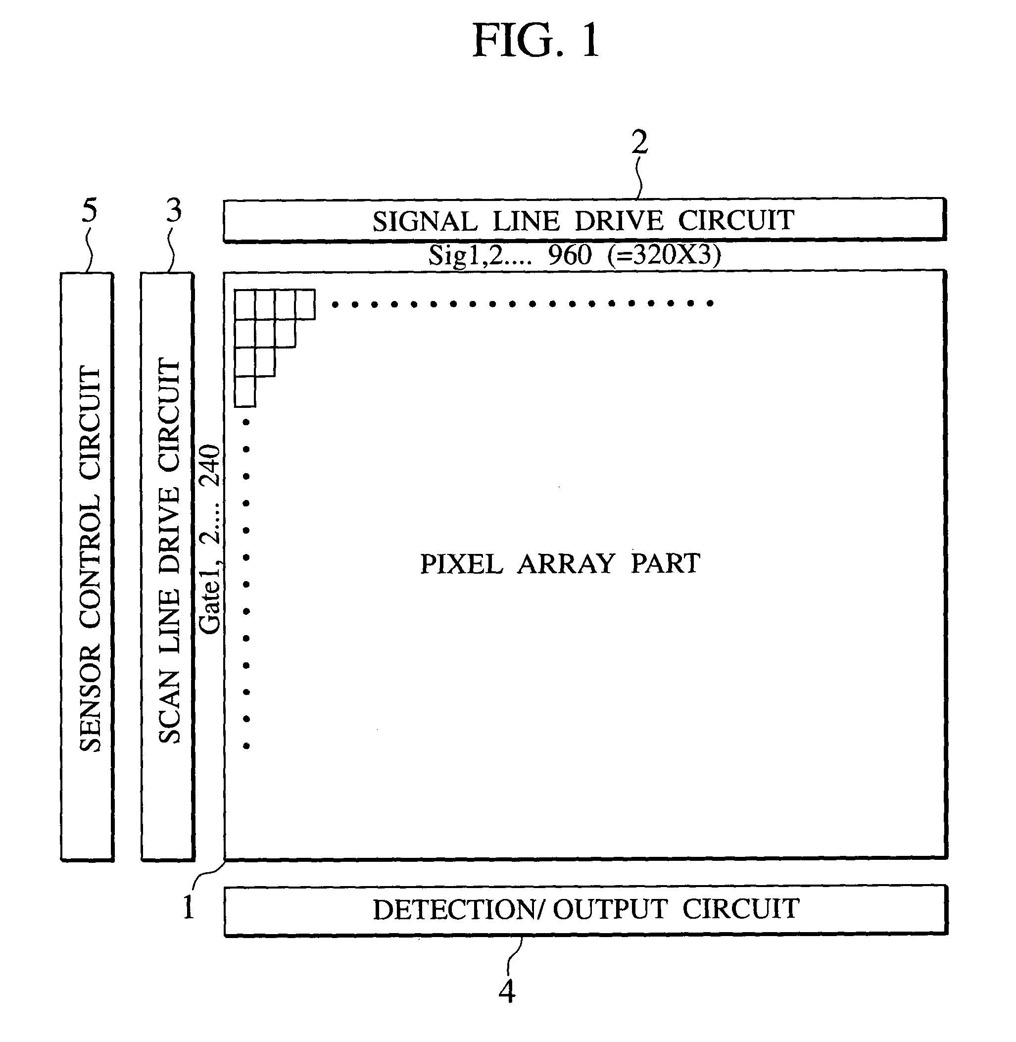
[0053]As shown in a circuit block diagram of FIG. 1, a display device of a first embodiment includes, on an insulating substrate made of glass: a pixel array part 1 in which pixels are disposed at the respective intersections of signal lines and scan lines; a signal line drive circuit 2 which drives the signal lines; a scan line drive circuit 3 which drives the scan lines; a detection / output circuit 4 which acquires and outputs an image; and a sensor control circuit 5 which controls sensors for image acquisition. This detection / output circuit 4 includes analog / digital conversion circuits for image acquisition and parallel / serial conversion circuits for output. These above-described circuits constitute an array substrate.

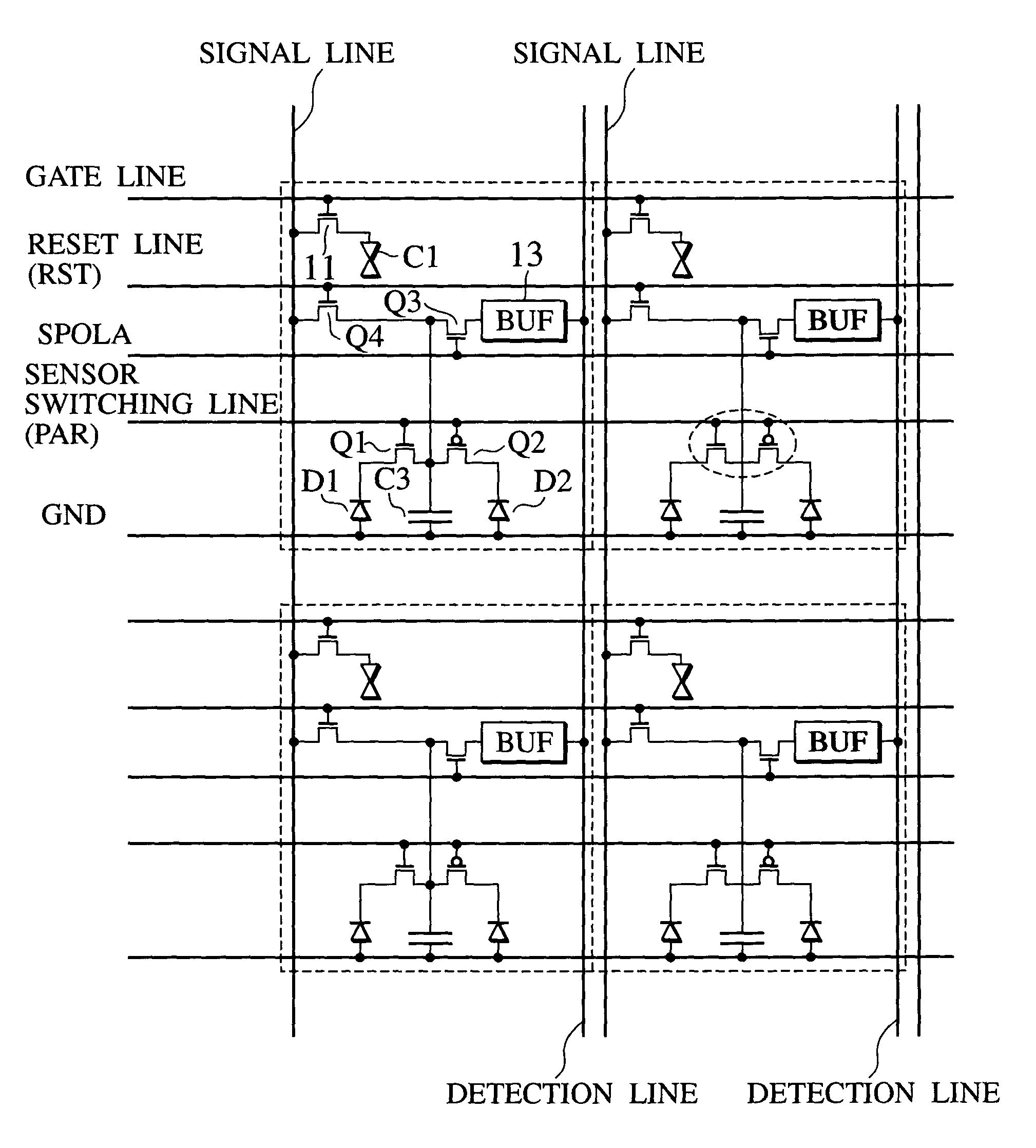
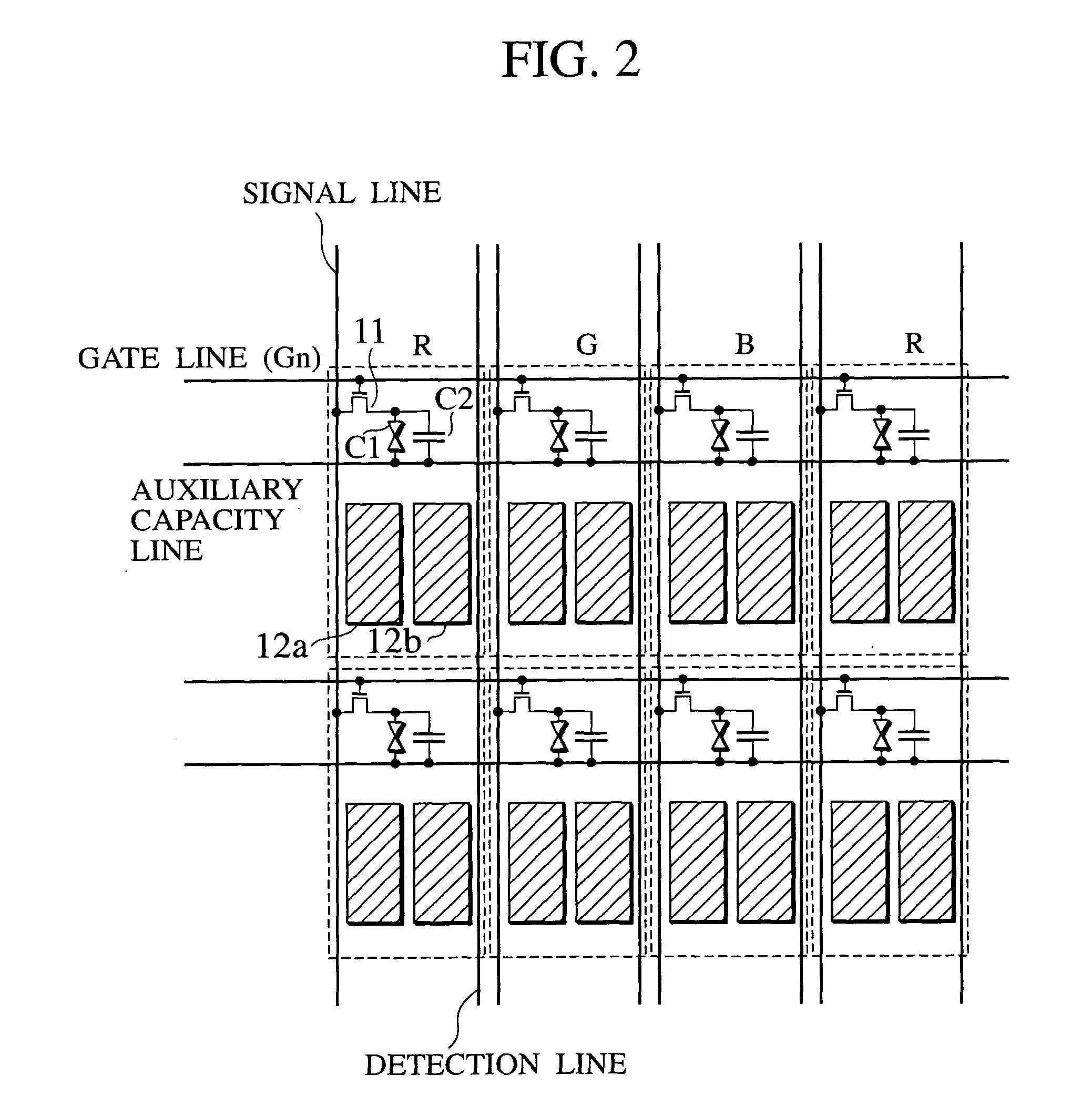
[0054]As shown in a detailed circuit block diagram of FIG. 2, the pixel array part 1 has: switching elements 11 for driving pixels, which are formed at the respective intersections of the signal lines and the scan lines (gate lines) that are instal...

second embodiment

2. Second Embodiment

[0096]As shown in a cross-sectional view of FIG. 14, in an optical sensor diode according to a second embodiment, a silicon film 102 is formed to have a thickness of about 150 nm on a glass insulating substrate 101 by plasma CVD. The silicon film 102 is formed of silicon nitride, silicon oxide or lamination thereof. On the silicon film 102, a semiconductor layer 110 made of polysilicon is formed so as to have a thickness of about 50 nm. This semiconductor layer 110 is formed by disposing a p region 111 with p-type impurities injected therein, an i region 112 including hardly any impurities and a n region 113 with n-type impurities injected therein adjacently to each other in this order. In the p region 111, boron is injected, for example, at a high concentration of about 1×10¹⁹ atm / cm3. In the n region 113, phosphorous is injected at a high concentration of about 1×10¹⁹ atm / cm3. The i region 112 may be a region to which boron or phosphorous is injected at a lower...

third embodiment

3. Third Embodiment

[0106]As shown in the circuit diagram of FIG. 19, in a circuit configuration of a third embodiment, a bias voltage Vnp is supplied to the cathode electrode 116 of the optical sensor diode 100 and a gate voltage Vgp is supplied to the gate electrode 114. The anode electrode 115 is connected to ground.

[0107]The graph of FIG. 20 shows current-voltage characteristics of the optical sensor diode 100 when a fixed voltage is applied as the gate voltage Vgp in the circuit diagram shown in FIG. 19. This graph shows a characteristic 405 in the case of irradiating no light onto the optical sensor diode 100 and a characteristic 406 in the case of irradiating light. This graph shows a good characteristic in which a current ratio of a current at the time of irradiating light (hereinafter referred to as an “irradiation current”) to a current at the time of no irradiation (hereinafter referred to as a “non-irradiation current”), which is irradiation current / non-irradiation curren...


PUM

PropertyMeasurementUnit
voltageaaaaaaaaaa
gate voltage Vgnaaaaaaaaaa
gate lengthaaaaaaaaaa

Abstract

In a manufacturing process of a display device, hydrogenation in an I layer of photodiodes D1 and D2 is progressed less than that in a channel portion of a pixel TFT, and a defect density due to dangling bonds not terminated in the I layer of the photodiodes D1 and D2 is made higher than a defect density in the channel portion of the pixel TFT. Thus, while suppressing a leakage current of the pixel TFT, the sensitivity of the photodiodes D1 and D2 to light is improved. Moreover, a gate electrode is provided above an i region of a pin-type optical sensor diode with an insulating film interposed therebetween. Thus, a gate voltage can control a threshold of a bias voltage when a current starts to flow into the optical sensor diode and a leakage current is prevented from flowing into the optical sensor diode.

Description

CROSS-REFERENCE TO RELATED APPLICATIONS[0001]This application is based upon and claims the benefit of priority from Japanese Patent Application No. 2002-254851 filed on Aug. 30, 2002 and No. 2002-281665 filed on Sep. 26, 2002; the entire contents of which are incorporated herein by reference.BACKGROUND OF THE INVENTION[0002]1. Field of the Invention[0003]The present invention relates to a technology for suppressing a leakage current at the time of image acquisition in a display device including an image acquisition function or in an image acquisition circuit.[0004]2. Description of the Related Art[0005]A liquid crystal display device includes: a pixel array part including pixels at respective portions where a plurality of signal lines and a plurality of scan lines intersect with each other; and drive circuits which drive the signal lines and the scan lines. Along with the recent advanced development of integrated circuit technologies, a process technology for forming a part of the d...

Claims


Application Information

Patent Timeline
Patent Type & Authority Patents(United States)
IPC IPC(8): G09G3/36G02F1/136H01L21/00H01L21/336H01L27/00H01L27/14H01L27/146H01L27/15H01L29/00H01L29/786H01L31/10H01L31/12H01R9/22
CPCH01L27/14609H01L27/14645H01L27/14692G02F2001/13312H01L31/125G02F1/13312G09G3/36
Inventor TADA, MASAHIRONAKAMURA, TAKASHITADA, NORIOYOSHIDA, MASAHIRO
Owner JAPAN DISPLAY CENTRAL CO LTD
Why Eureka
Try Eureka