Semiconductor storage apparatus or semiconductor memory module

a technology of semiconductor memory and storage apparatus, which is applied in the direction of static storage, digital storage, instruments, etc., can solve the problems of increasing the overall time for rewriting operation, unable to correct rewriting the desired information, etc., and achieve stable low-current operation and high rewriting data transfer efficiency

Active Publication Date: 2012-06-21
HITACHI LTD
View PDF2 Cites 5 Cited by
  • Summary
  • Abstract
  • Description
  • Claims
  • Application Information

AI Technical Summary

Benefits of technology

[0018]In view of the above problems with the related art, the present invention has the object of providing technology for achieving an

Problems solved by technology

However, the present inventors perceived that this type of technology for rewriting data onto phase-change memories also contained the following problems.
This electrical current value is on a widely different scale than for NAND type flash memories and so during simultaneous writing of several hundred bytes to several kilobytes of data

Method used


Image

  • Semiconductor storage apparatus or semiconductor memory module
  • Semiconductor storage apparatus or semiconductor memory module
  • Semiconductor storage apparatus or semiconductor memory module

Examples


first embodiment

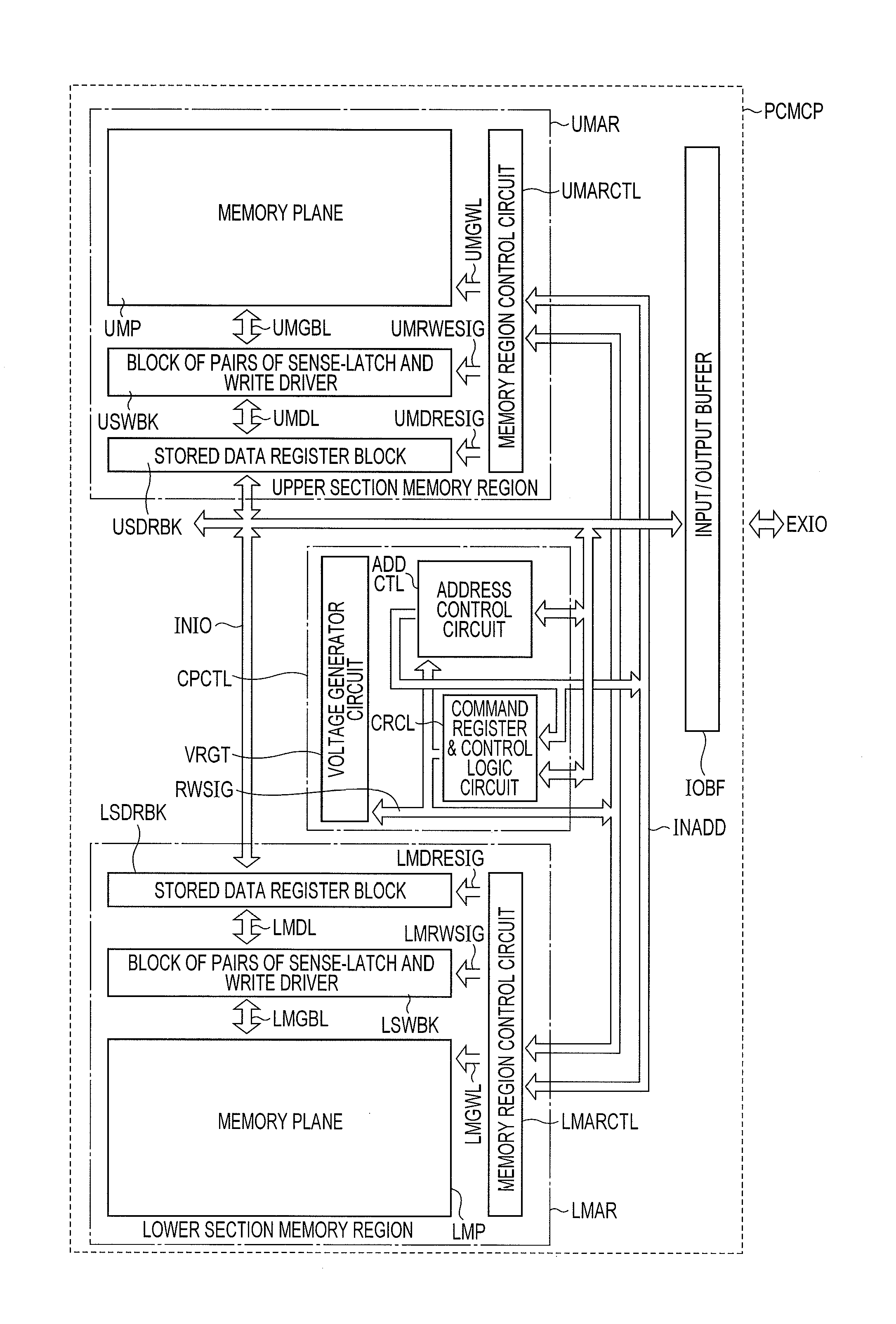
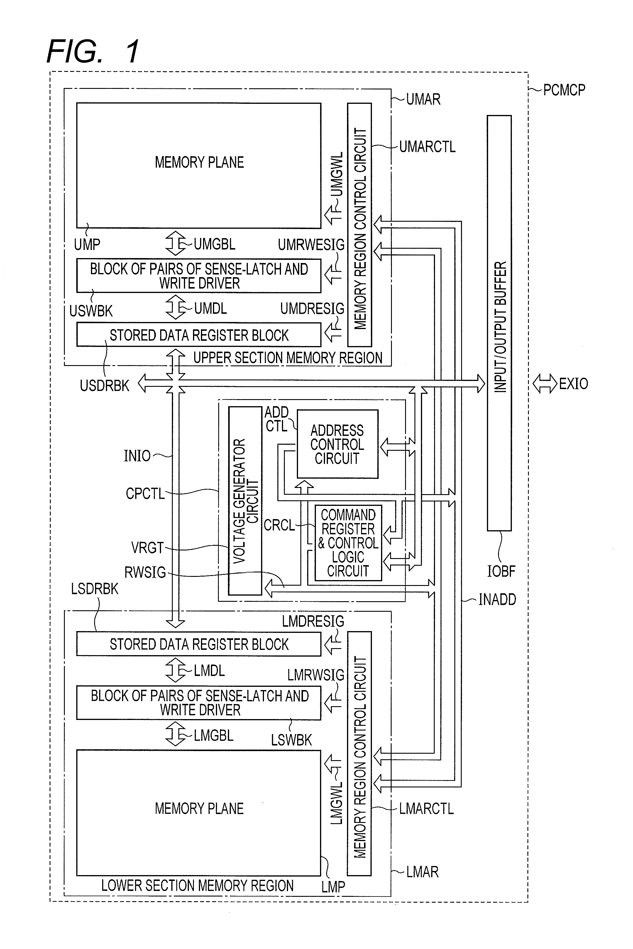
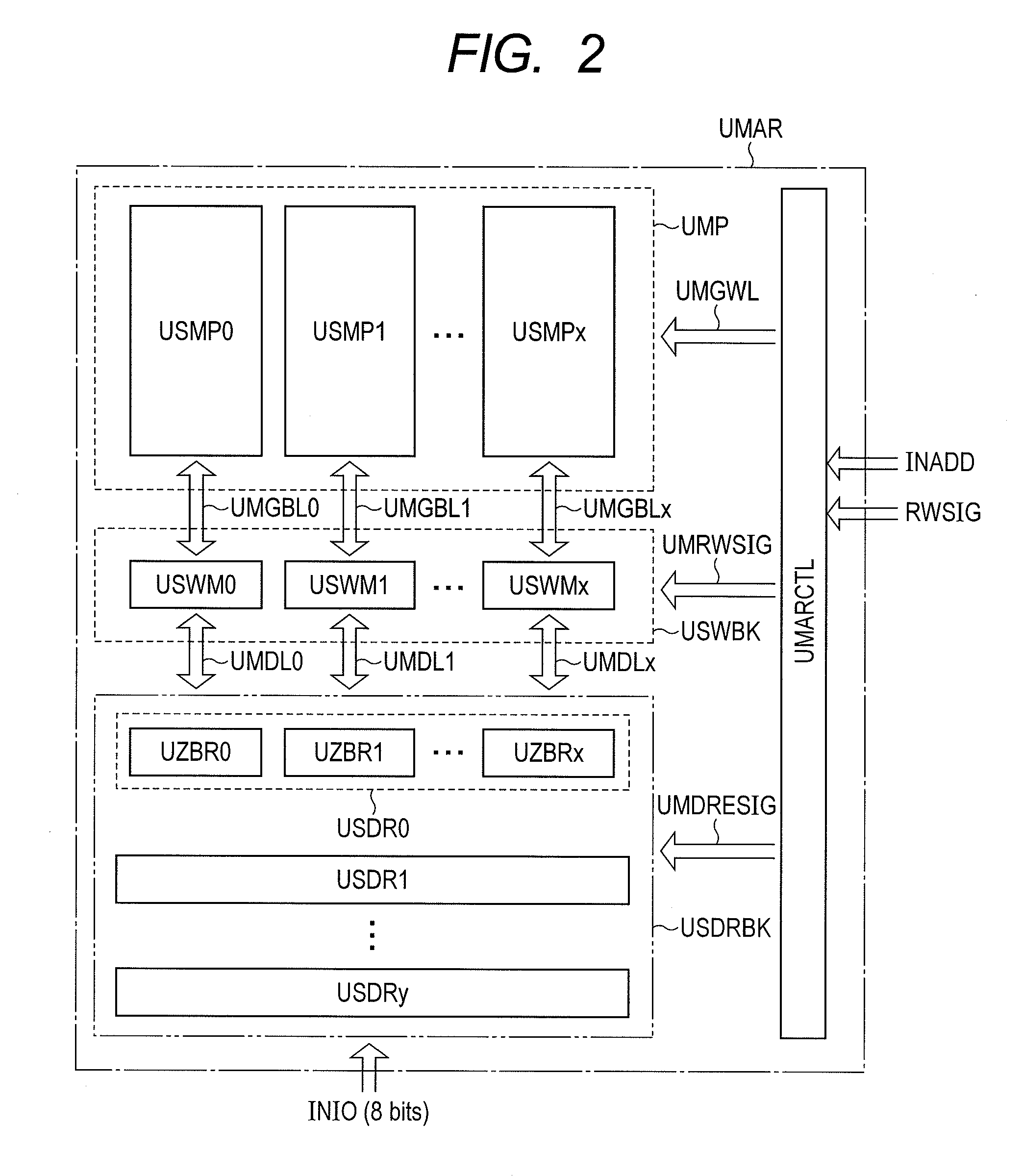
[0057]FIG. 1 is a block diagram showing one example of the structure of an essential circuit section of the phase-change memory chip of the first embodiment of the present invention. FIG. 2 is a block diagram showing one example of the structure of an essential circuit section of the upper section memory region on phase-change memory chip in FIG. 1. FIG. 3 is a block diagram showing one example of the structure of the wiring coupling the essential circuit section in the upper section memory region in FIG. 2. FIG. 4 is a wiring diagram showing one example of the specific structure of the essential circuit section in the upper section memory region of FIG. 3. FIG. 5 is a drawing showing one example of the structure of the memory cell in the upper section memory region of FIG. 3. FIG. 6 is a timing chart showing one example of the operation of the two kilobyte rewrite operation in the phase-change memory chip of FIG. 1. FIG. 7 is a timing chart showing one example of the receive operat...

second embodiment

[0186]FIG. 12 is a timing chart showing one example of the phase relation between the verify read and the rewrite operation in the rewrite operation sequence on the phase-change memory chip in the second embodiment of the present invention. FIG. 13 is a timing chart showing one example of the detailed operation in the upper section memory region in the rewrite, operation sequence described in FIG. 12. FIG. 14 is a drawing showing one example of the detailed operation in the lower section memory region in the rewrite operation sequence described in FIG. 13.

Brief Overview of the Invention

[0187]A second point of the present invention is comprised of a first and a second memory region (upper section memory region UMAR, lower section memory region LMAR). The first memory region includes a first and a second memory plane (sub-plane USMP0, sub-plane USMP1) containing multiple memory cells arranged in a matrix; and a first and a second blocks of pairs of sense-latch and write driver (small-...

third embodiment

[0208]FIG. 15 is a block diagram showing one example of the structure of the semiconductor memory module utilizing the phase-change memory chip in the third embodiment of the present invention.

Brief Overview of the Invention

[0209]A third point of the invention is a semiconductor memory module (semiconductor memory module PCMMDL) comprised of multiple memory chips (phase-change memory chips PCMCP0 through PCMCP3), and a controller chip (controller block CTLRBLK) for controlling the operation of the memory chips.

[0210]The memory chips are comprised of a first and a second memory region (upper section memory region UMAR, lower section memory region LMAR). The first memory region includes a first and a second memory planes (sub-plane USMP0, sub-plane USMP1) containing multiple memory cells arranged in a matrix; and a first and a second blocks of pairs of sense-latch and write driver (small-scale blocks of pairs of sense-latch and write driver USWM0, USWM1) to read and to write informati...


PUM


Abstract

A semiconductor storage apparatus provides a large capacity phase-change memory possessing high speed operation, low electrical current, and high-reliability. During the period that a read-out start signal is activated in the memory region control circuit and the block of pairs of sense-latch and write driver is performing the verify read in the upper section memory region; the write enable signals in the memory region control circuit are activated and the block of pairs of sense-latch and write driver perform rewrite operation of the data in the lower section memory region. This type of operation allows cancelling out the time required for the verify read and the time required for the time-division write operation by performing the verify read in one memory region, while performing time-division rewrite in other memory region, to achieve both higher reliability rewrite operation along with suppressing the rewrite operation peak electrical current.

Description

CLAIM OF PRIORITY[0001]The present application claims priority from Japanese patent application JP 2010-280871 filed on Dec. 16, 2010, the content of which is hereby incorporated by reference into this application.FIELD OF THE INVENTION[0002]The present invention relates to technology for rewriting data in non-volatile semiconductor memories, and relates in particular to technology effective for storage devices containing memory cells comprised of elements with resistance values that differ according to the stored data.BACKGROUND OF THE INVENTION[0003]NAND type flash memories are currently exhibiting amazing growth as a memory for holding non-volatile storage of programs and data. NAND type flash memories include features such as large capacity and also high-speed data transfer. To achieve a large capacity memory, a NAND string structure is utilized that improves the memory cell usage rate by reducing the surface area coupled to the bit lines and memory cells. Large capacity was als...

Claims


Application Information

Patent Timeline
IPC IPC(8): G11C11/00G11C7/00
CPCG11C7/1039G11C7/1042G11C7/22G11C13/0004G11C13/0007G11C13/004G11C2211/5624G11C13/0064G11C13/0069G11C2207/2209G11C2207/2245G11C2211/5623G11C13/0061
Inventor HANZAWA, SATORU
Owner HITACHI LTD
Why Eureka
Try Eureka