Method of manufacturing image sensor for reducing dark current

a technology of image sensor and dark current, which is applied in the direction of semiconductor devices, diodes, radiation control devices, etc., can solve the problems of preventing the dangling bond from being removed and suppressing the excessive generation of dark current, so as to prevent the deterioration of picture quality

Inactive Publication Date: 2004-12-28
INTELLECTUAL VENTURES II
View PDF8 Cites 31 Cited by
  • Summary
  • Abstract
  • Description
  • Claims
  • Application Information

AI Technical Summary

Benefits of technology

The disclosed method provides a method of manufacturing an image sensor capable of preventing picture quality deterioration, which is caused by a dark current.

Problems solved by technology

Moreover, in the conventional method, as shown in FIG. 2, the protection layer 25 is formed only with an oxide layer, therefore, it is impossible to remove the dangling bonds and to suppress the excessive generation of the dark current.

Method used


Image

  • Method of manufacturing image sensor for reducing dark current
  • Method of manufacturing image sensor for reducing dark current
  • Method of manufacturing image sensor for reducing dark current

Examples


Embodiment Construction

Hereinafter, a method for manufacturing an image sensor for reducing a dark current according to the disclosed method will be described in detail referring to the accompanying drawings.

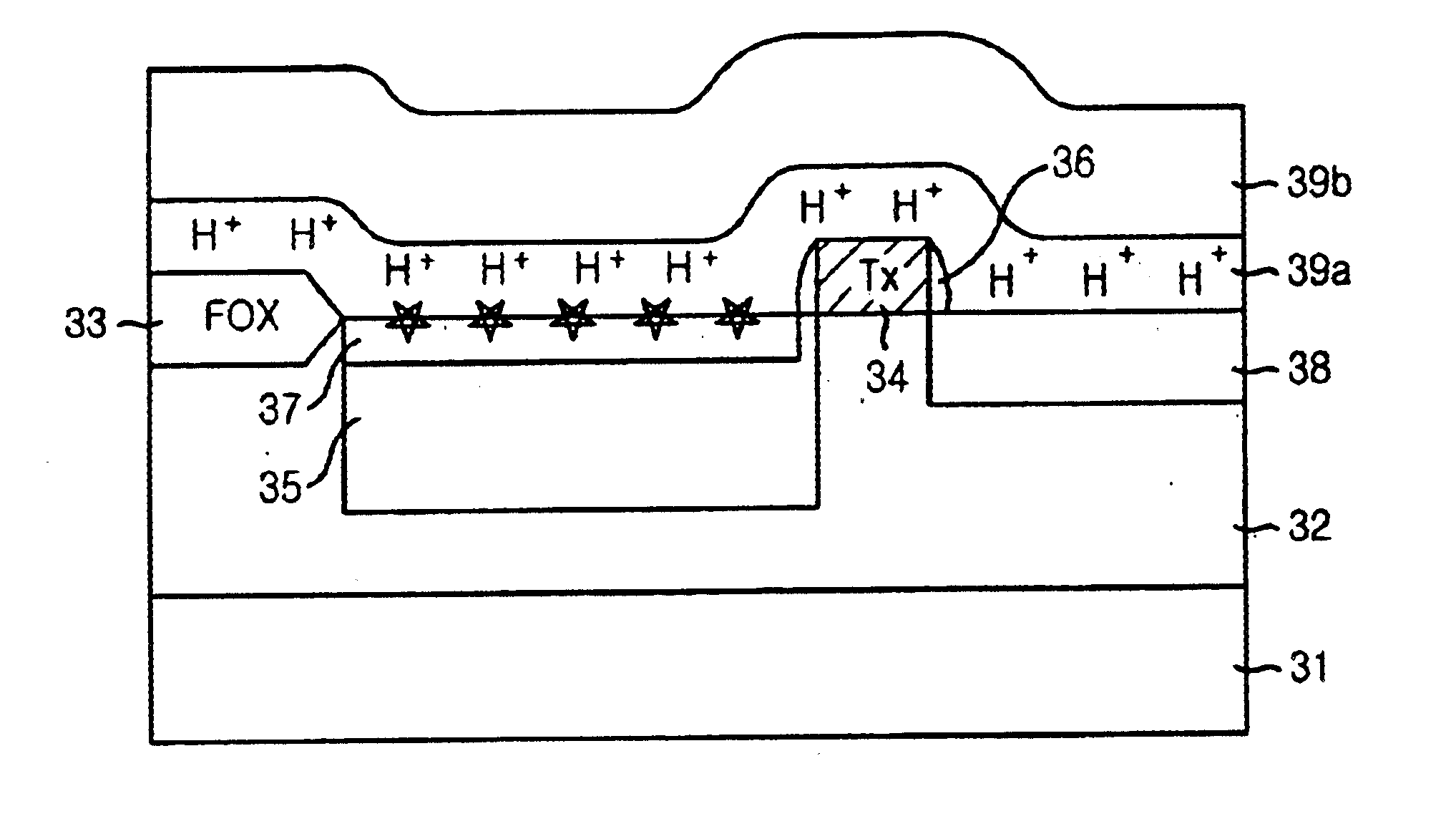
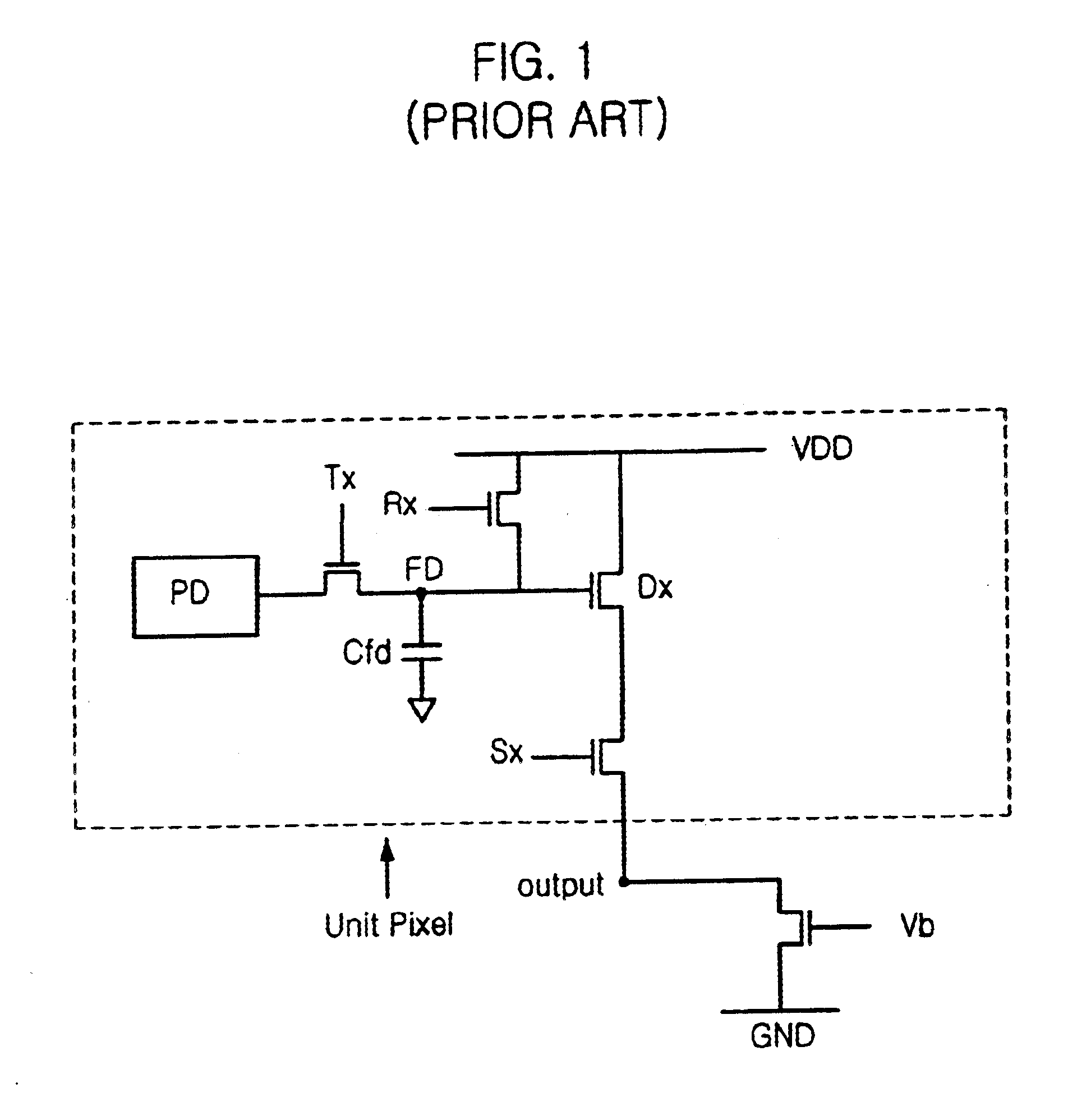
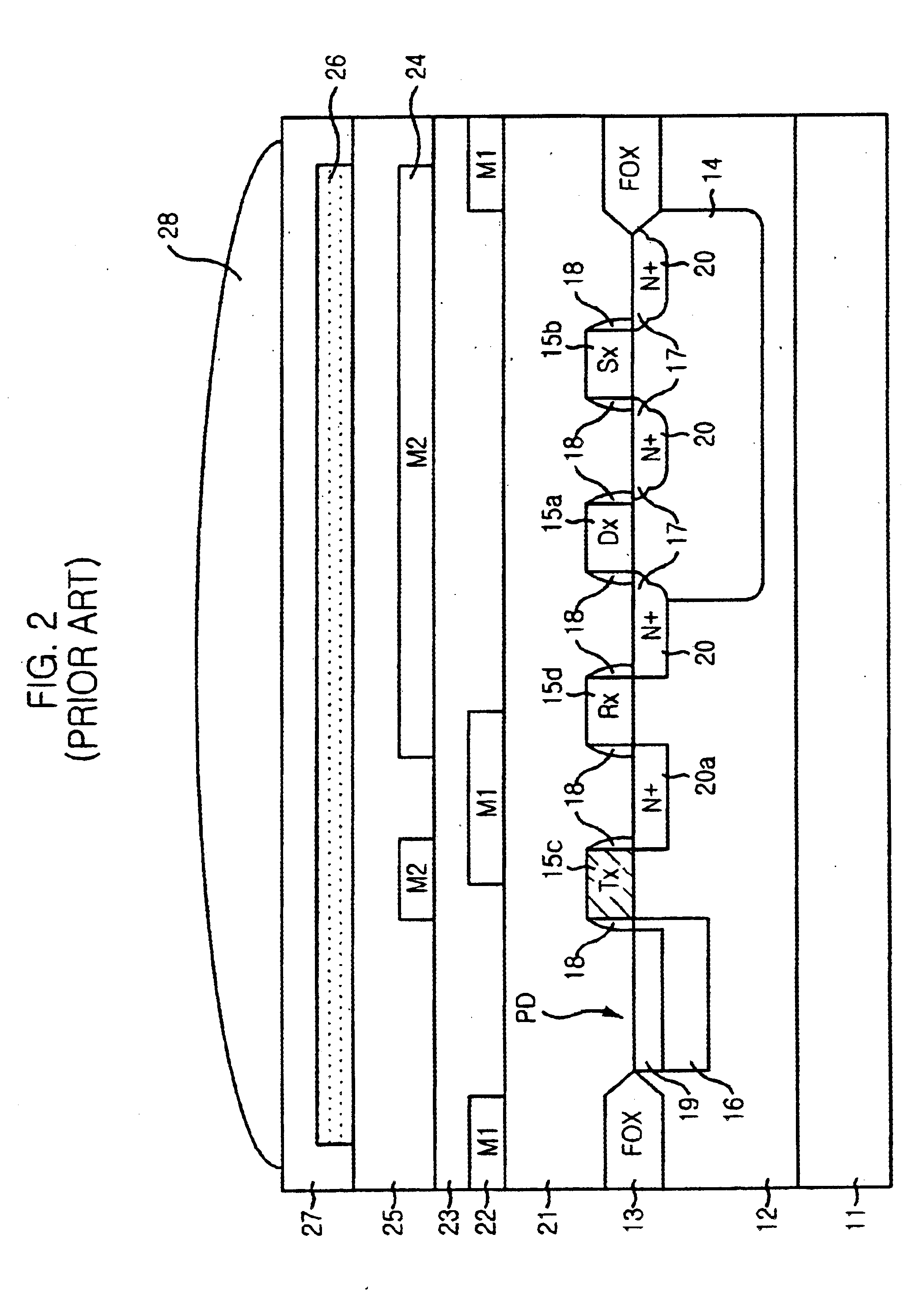
FIGS. 4A to 4C are cross-sectional views showing a method of manufacturing a complementary metal oxide semiconductor (CMOS) image sensor in accordance with the disclosed method. In these figures, a reset transistor, a drive transistor and a select transistor are omitted.

Referring to FIG. 4A, a p-epitaxial layer 32 is grown on a p.sup.+ -substrate 31. Herein, the p.sup.+ -substrate 31 is doped with a high concentration of p-type dopant and the p-epitaxial layer 32 is doped with a low concentration of p-type dopant. After growing the p-epitaxial layer 32, a field oxide layer 33 for separating unit pixels is formed in a predetermined region of the p-epitaxial layer 32 by using a local oxidation of silicon (LOCOS) method.

Thereafter, a p-well (not shown) is formed in a predetermined region of the p-epitaxi...


PUM


Abstract

The disclosed method provides a method capable of removing dangling bonds generated on a surface of photodiode. The method includes steps of: forming a photodiode in a semiconductor substrate; forming a transfer transistor, a reset transistor, a drive transistor and a select transistor on the semiconductor substrate; forming a first interlayer insulating layer on the semiconductor substrate, wherein the first interlayer insulating layer contains hydrogen ions; forming a second interlayer insulating layer on the first interlayer insulating layer; and flattening the second interlayer insulating layer by flowing and simultaneously diffusing the hydrogen ions into a surface of the photodiode.

Description

BACKGROUND OF THE DISCLOSURE1. Field of the DisclosureThe disclosed method relates to a method for manufacturing a semiconductor device; and, more particularly, to a method for manufacturing a complementary metal oxide semiconductor (CMOS) image sensor.2. Description of the Prior ArtGenerally, in a charge couple device (CCD) or a complementary metal oxide semiconductor (CMOS) image sensor, a photodiode (PD), namely a light sensing area, changes an incident light in accordance with each wavelength into an electric signal. An ideal case is that quantum efficiency is one for all wavelengths of light, that is, all the incident light gathered in the photodiode is converted into electric signal.FIG. 1 is an equivalent circuit diagram of a general CMOS image sensor unit pixel. Referring to FIG. 1, the equivalent circuit includes one photodiode (PD) and four n-channel metal oxide semiconductor (NMOS) transistors (Tx, Rx, Dx, and Sx). The four NMOS transistors are comprised of a transfer tra...

Claims


Application Information

Patent Timeline
Patent Type & Authority Patents(United States)
IPC IPC(8): H01L27/146H01L21/70H01L21/02H01L21/768H01L21/3105H01L31/10
CPCH01L21/31051H01L21/76819H01L27/14689H01L27/14609H01L27/14698H01L27/14643H01L27/14627H01L27/146
Inventor LEE, JU-IL
Owner INTELLECTUAL VENTURES II
Why Eureka
Try Eureka