Electrical passivation of silicon-containing surfaces using organic layers

a technology of organic layers and silicon-containing surfaces, applied in the direction of thermoelectric devices, basic electric elements, solid-state devices, etc., can solve the problems of surface states that form electrical defects, poor electrical properties of such surfaces, and site of electrical defects of crystalline solids, so as to improve the electrical properties of electrical devices, improve the electrical properties of silicon-based electronic materials, and reduce the effect of dangling bonds

Inactive Publication Date: 2009-02-17
CALIFORNIA INST OF TECH
View PDF18 Cites 29 Cited by
  • Summary
  • Abstract
  • Description
  • Claims
  • Application Information

AI Technical Summary

Benefits of technology

[0012]An organic passivating layer that is chemically bonded to a silicon-containing surface may be used to improve the electrical properties of silicon-based electronic materials and to improve the properties of electrical devices resulting from the use of such materials. In different embodiments, the organic passivating layer may remain within finished devices to reduce dangling bonds, improve carrier lifetimes, decrease surface recombination velocities, allow controlled spacing on the molecular scale between various other layers in the device, or to increase the electronic efficiencies of the surfaces and devices. In other embodiments, the organic passivating layer may be used as a protective sacrificial layer which ultimately reduces contact resistance or which ultimately reduces the resistance of doped regions in the device.

Problems solved by technology

In general, surfaces of crystalline solids are sites of electrical defects because the atoms at the surface do not experience the same bonding as atoms in the bulk of the crystalline material.
Surface states that form electrical defects are a particularly important issue for silicon-based electrical devices.
The poor electrical properties of such surfaces are manifested in many physical properties of electronic devices formed form such materials.
However, the H-terminated silicon-containing surface is not stable in the presence of air.
Similarly, halogens have been used to form halogen-covered silicon-containing surfaces, but such surfaces likewise suffer from a similar instability in air.
In addition, such surfaces have poor surface recombination velocities in contact with air, allowing electrons which should be flowing as electrical current to recombine with holes thereby providing inferior electrical properties of the resulting devices and device structures.
However, silicon dioxide is an electrical insulator and often the thickness of this insulator is too great for formation of certain electrical device structures, in which little or no silicon oxide is desired on the silicon-containing surface.
Formation of silicon oxides requires high temperatures, and often these high temperatures interfere with previous device processing acts which cannot tolerate high processing temperatures.
The exposure to high temperature required for form the silicon dioxide, therefore, produces degraded performance from the resulting electrical device or requires an alteration in the flow of process acts to form the final desired device structure.
Also, during formation of electrical devices, formation of too much silicon oxide or exposure of the surface to undesired contaminants may adversely affect device performance.
If too much native silicon oxide is formed, a subsequent contact metalization may make poor electrical contact, if any, to the substrate.
Likewise, too much silicon oxide may prevent diffusion of dopant from an overlying layer into the substrate.
Unfortunately, queue times are difficult to implement in manufacturing.
A backlog of work at a piece of equipment or equipment downtime may make queue time compliance very difficult to administer.

Method used


Image

  • Electrical passivation of silicon-containing surfaces using organic layers
  • Electrical passivation of silicon-containing surfaces using organic layers
  • Electrical passivation of silicon-containing surfaces using organic layers

Examples


Embodiment Construction

[0030]Reference is now made in detail to the exemplary embodiments of the invention, examples of which are illustrated in the accompanying drawings. Wherever possible, the same reference numbers will be used throughout the drawings to refer to the same or like parts (elements).

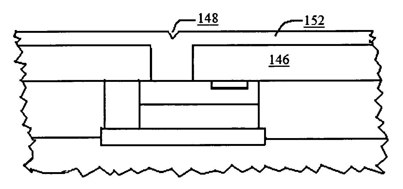
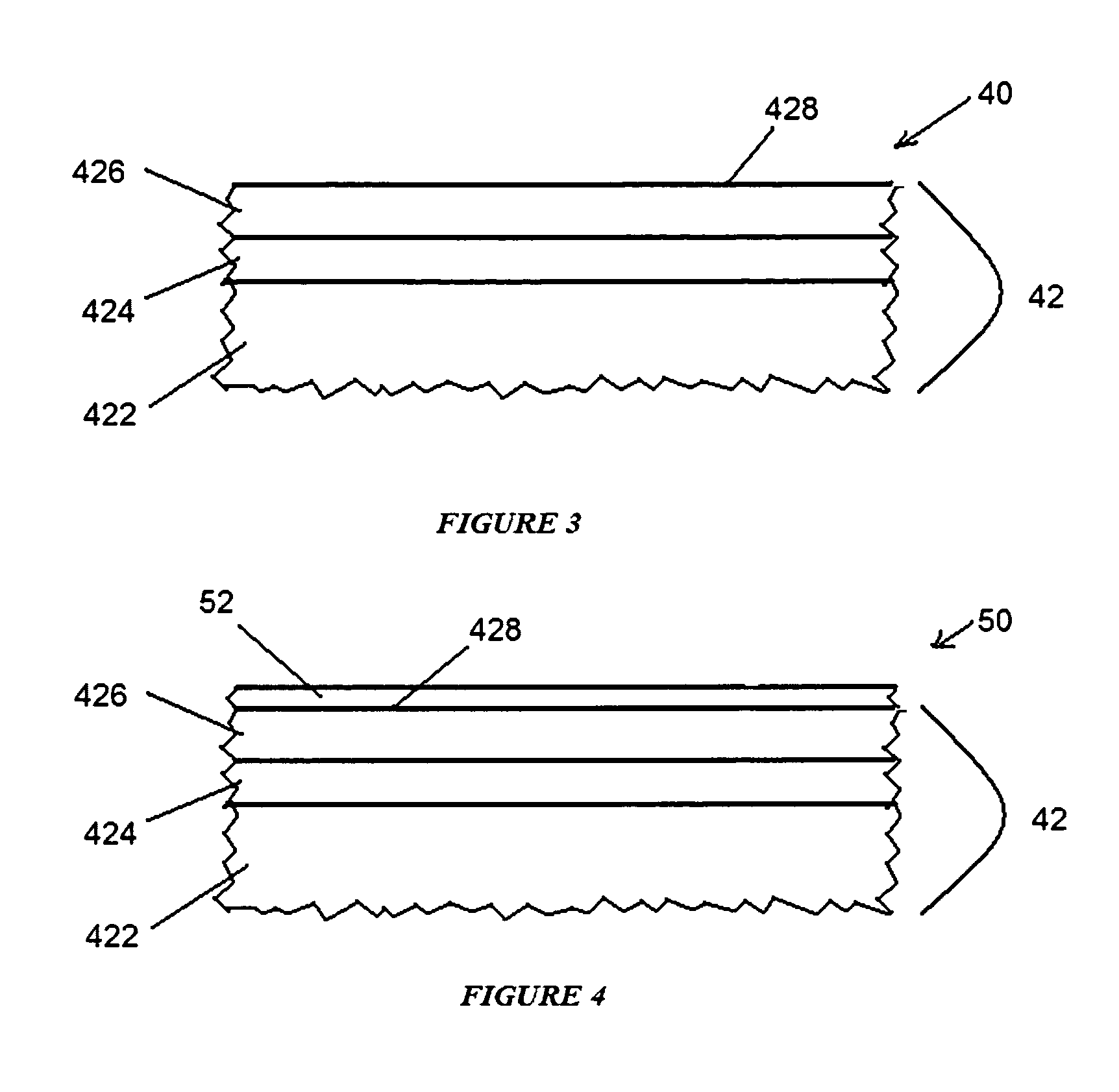
[0031]Electrical structures and devices may be formed and include an organic passivating layer that is chemically bonded to silicon to improve the electrical properties of electrical devices. In different embodiments, the organic passivating layer may remain within finished devices to reduce dangling bonds, improve carrier lifetimes, decrease surface recombination velocities, increase capacitance, or provide improvements in other electronic properties, such as voltage. In other embodiments, the organic passivating layer may be used as a protective sacrificial layer and reduce the contact resistance or reduce the resistance of doped regions.

[0032]Attention is now directed to specific embodiments. The semiconduc...


PUM


Abstract

Electrical structures and devices may be formed and include an organic passivating layer that is chemically bonded to a silicon-containing semiconductor material to improve the electrical properties of electrical devices. In different embodiments, the organic passivating layer may remain within finished devices to reduce dangling bonds, improve carrier lifetimes, decrease surface recombination velocities, increase electronic efficiencies, or the like. In other embodiments, the organic passivating layer may be used as a protective sacrificial layer and reduce contact resistance or reduce resistance of doped regions. The organic passivation layer may be formed without the need for high-temperature processing.

Description

RELATED APPLICATIONS[0001]This application claims priority under 35 U.S.C. § 119(e) to U.S. patent application Ser. No. 60 / 217,749 entitled “Electrical Passivation of Silicon-containing surfaces Using Organic Layers” by Lewis et al. filed Jul. 12, 2000. This application is also related to U.S. patent application Ser. No. 09 / 305,125 entitled “Stabilization of Si Photoanodes in Aqueous Electrolytes Through Surface Alkylation” by Lewis at al. filed May 4, 1999. Both applications are assigned to the current assignee hereof and incorporated herein by reference.STATEMENT AS TO FEDERALLY SPONSORED RESEARCH AND DEVELOPMENT[0002]The U.S. Government has certain rights in this invention pursuant to Grant No. CHE-9974562 awarded by the National Science Foundation.FIELD OF THE INVENTION[0003]This invention relates in general to electrical structures and processes for forming electrical devices, and more particularly, to electrical structures and processes for forming electrical devices having or...

Claims


Application Information

Patent Timeline
Patent Type & Authority Patents(United States)
IPC IPC(8): H01L21/4763H01L21/285H01L21/306H01L21/312H01L21/768H01L23/29H01L23/31H01L31/0216
CPCH01L21/28512H01L21/28537H01L21/306H01L21/312H01L21/3128H01L21/76807H01L21/76814H01L23/293H01L23/3171H01L31/02167H01L2221/1063H01L2924/12044H01L2924/13091H01L2924/19041Y02E10/50H01L2924/0002H01L2924/00H01L21/02118
Inventor LEWIS, NATHAN S.ROYEA, WILLIAM
Owner CALIFORNIA INST OF TECH
Why Eureka
Try Eureka