CMOS image sensor with a low-power architecture

a low-power architecture and image sensor technology, applied in the field of low-power architectures of cmos image sensors, can solve the problems of extremely important power consumption, and achieve the effect of reducing power and saving power

Inactive Publication Date: 2006-06-27
ROUND ROCK RES LLC
View PDF25 Cites 37 Cited by
  • Summary
  • Abstract
  • Description
  • Claims
  • Application Information

AI Technical Summary

Benefits of technology

[0002]The present application teaches an image sensor architecture with reduced power. According to an aspect, different areas of the image sensor are optimized separately, to save power.

Problems solved by technology

Overall power consumption may be extremely important in camera systems and other type systems which use image sensors.
However, there is often a direct trade-off between the amount of power that is consumed, and the quality of the image or images obtained by the sensor.

Method used


Image

  • CMOS image sensor with a low-power architecture
  • CMOS image sensor with a low-power architecture
  • CMOS image sensor with a low-power architecture

Examples


Embodiment Construction

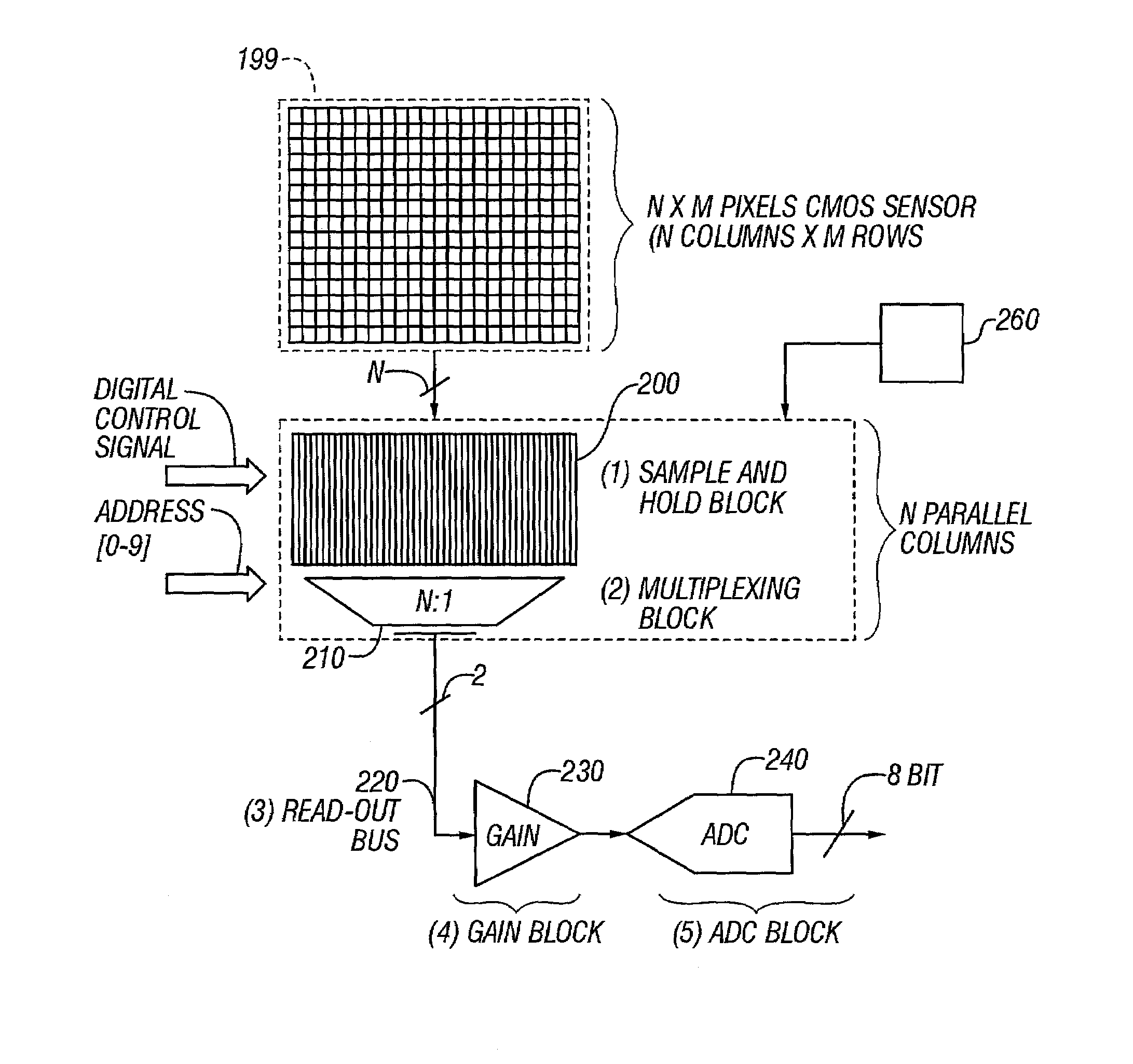
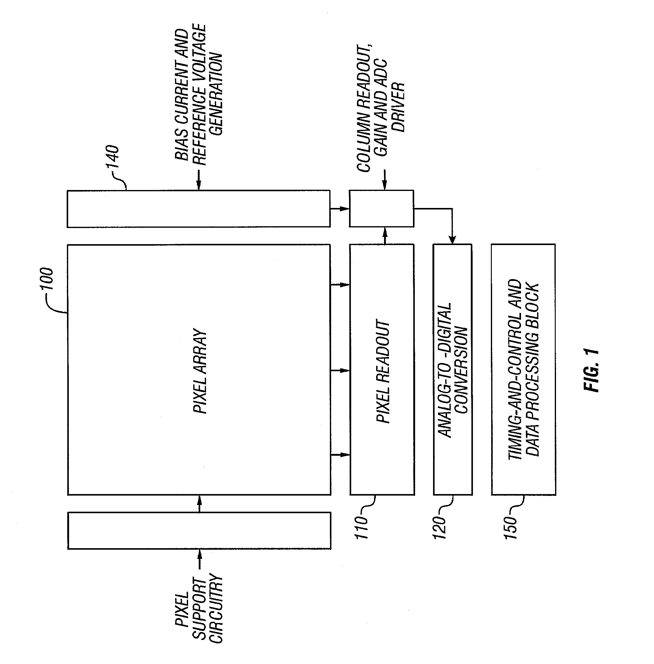
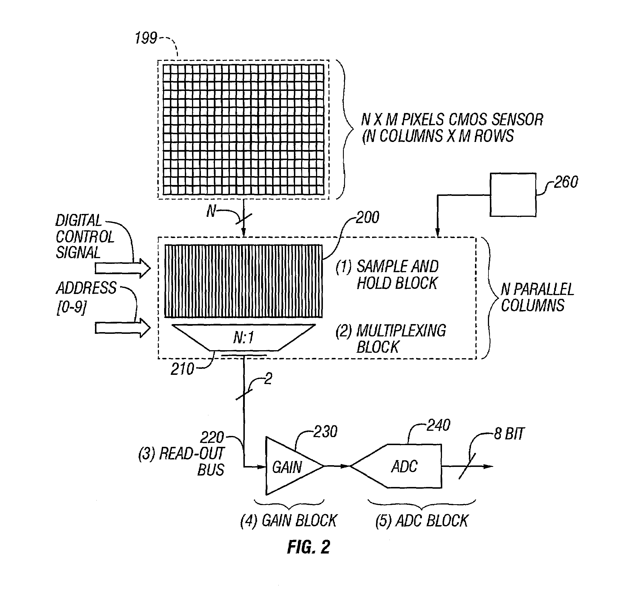
[0014]FIG. 1 shows a basic block diagram of a CMOS image sensor. The CMOS image sensor is functionally a number of different blocks. According to the present system, different areas of this CMOS image sensor may be optimized separately in order to save power. Specifically, the column readout, gain and output drive, may be separately optimized.

[0015]Block 100 includes the pixel array and its support circuitry, which can include the pixel selection circuitry, and bias current and reference voltage generation elements.

[0016]Block 110 includes the pixel readout circuitry, which may include the column readout circuitry, the gain circuits, and the A / D converter driving circuits.

[0017]The A / D conversion itself is carried out by block 120 which can include an array of A / D converters of any type, and may be successive approximation A / D converters, or other kinds as described herein.

[0018]The bias current and reference voltage generation block 140 produces specific voltages for operation of t...


PUM


Abstract

A system of reducing power consumption in and active pixels sensor. The sensor is broken into different blocks, and each of the blocks is individually optimized. The optimization may include minimizing the parasitic capacitance on the readout bus, turning off biases when not in use, and operating in a way that minimizes static power consumption of different elements such as A/D converters.

Description

BACKGROUND OF INVENTION[0001]Overall power consumption may be extremely important in camera systems and other type systems which use image sensors. Reduction of power consumption can prolong battery life, and can correspondingly allow smaller devices with smaller batteries or fewer batteries. However, there is often a direct trade-off between the amount of power that is consumed, and the quality of the image or images obtained by the sensor.SUMMARY OF INVENTION[0002]The present application teaches an image sensor architecture with reduced power. According to an aspect, different areas of the image sensor are optimized separately, to save power.BRIEF DESCRIPTION OF DRAWINGS[0003]These and other aspects will now be described in detail with reference to the accompanying drawings, wherein:[0004]FIG. 1 shows a basic block diagram of an active pixel sensor;[0005]FIG. 2 shows a block diagram of the readout chain for an active pixel sensor;[0006]FIG. 3 shows a single column parallel element...

Claims


Application Information

Patent Timeline
Patent Type & Authority Patents(United States)
IPC IPC(8): H04N5/225H01L27/00H03M1/66H04N3/14H04N5/335H04N9/083H04N5/351H04N5/374H04N5/378
CPCH04N3/1512H04N5/335H04N5/23241H04N25/76H04N25/75
Inventor BARNA, SANDOR L.ROSSI, GUISEPPECHO, KWANG-BOPANICACCI, ROGER
Owner ROUND ROCK RES LLC
Why Eureka
Try Eureka