Systems for inspection of patterned or unpatterned wafers and other specimen

a technology of patterned or unpatterned wafers and specimens, applied in the field of systems and methods for specimen inspection, can solve the problems of single detector being saturated, not yielding signals that can be analyzed, and tools generally not being able to inspect patterned wafers

Active Publication Date: 2006-06-27
KLA TENCOR TECH CORP
View PDF33 Cites 207 Cited by
  • Summary
  • Abstract
  • Description
  • Claims
  • Application Information

AI Technical Summary

Problems solved by technology

Since these tools are optimized for inspecting unpatterned wafers, these tools are generally not capable of inspecting patterned wafers for a number of reasons.
As such, the single detector may become saturated and, consequently, will not yield signals that can be analyzed for defect detection.
In addition, even if the single detector does not become saturated, the light scattered from patterns or other features on the wafer can not be separated from other scattered light thereby hindering, if not preventing, defect detection based on the other scattered light.
Although inspection of unpatterned wafers, or “monitor wafers,” which have been run through a process tool, may be

Method used


Image

  • Systems for inspection of patterned or unpatterned wafers and other specimen
  • Systems for inspection of patterned or unpatterned wafers and other specimen
  • Systems for inspection of patterned or unpatterned wafers and other specimen

Examples


Embodiment Construction

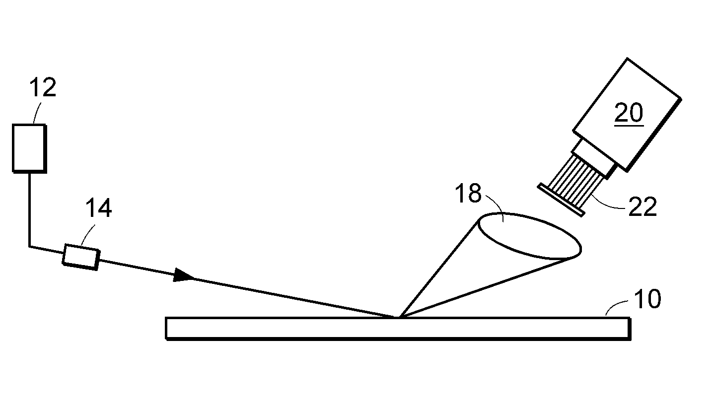
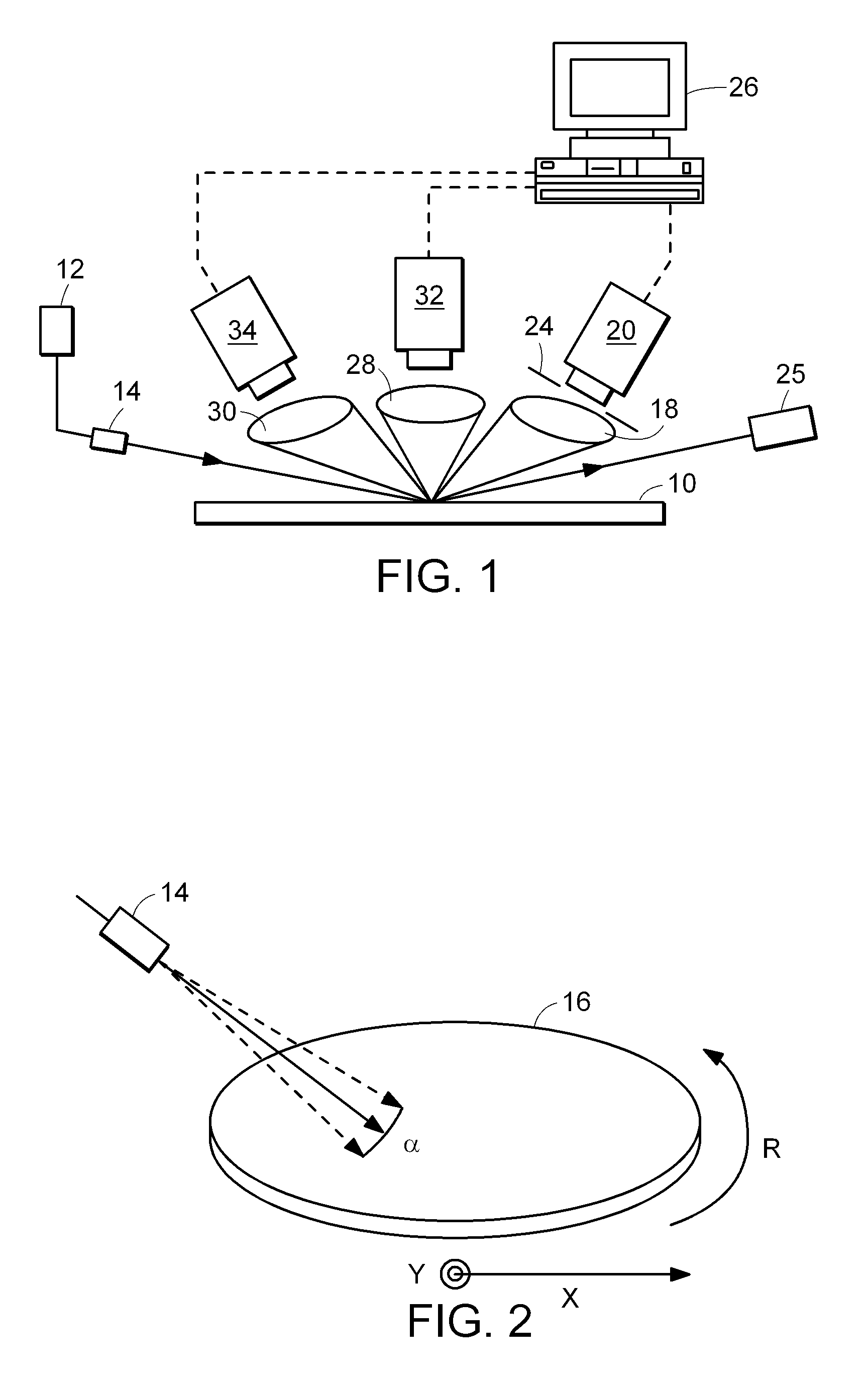
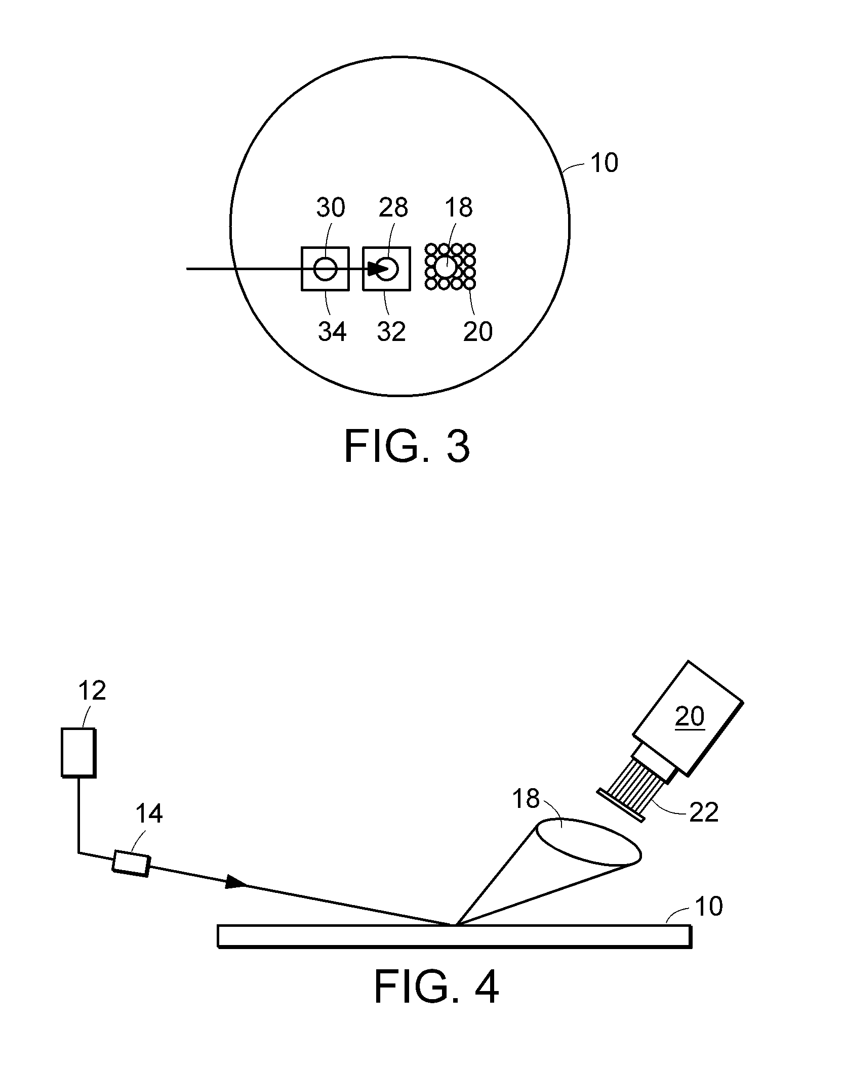
[0035]As used herein, the term “defect” generally refers to an abnormality formed on or within a specimen that may adversely affect the performance or functionality of a device formed on the specimen (i.e., reduce a characteristic such as speed or cause a device failure that may or may not cause a device to be non-working) or additional devices formed on the specimen if the cause is not fixed. Defects may be caused by individual process marginalities, process integration marginalities, or interactions between multiple processes. For example, a defect may be contamination on a specimen, abnormal structures on the specimen, damage to the specimen, subsurface pits or crystal originated pits (COPS), subsurface voids, or microscopic scratches. Contamination may include, but is not limited to, particles, fibers, or residual material remaining on a specimen after a process step. Contamination may also include organic or inorganic material such as a resist, a dielectric material, and / or a c...


PUM


Abstract

Systems for inspection of patterned and unpatterned wafers are provided. One system includes an illumination system configured to illuminate the specimen. The system also includes a collector configured to collect light scattered from the specimen. In addition, the system includes a segmented detector configured to separately detect different portions of the light such that azimuthal and polar angular information about the different portions of light is preserved. The detector may also be configured to produce signals representative of the different portions of the light. The system may also include a processor configured to detect defects on the specimen from the signals. In another embodiment, the system may include a stage that is configured to rotate and translate the specimen. In one such embodiment, the system may also include an illumination system configured to scan the specimen in a wide scan path during rotation and translation of the specimen.

Description

BACKGROUND OF THE INVENTION[0001]1. Field of the Invention[0002]This invention generally relates to systems and methods for inspection of a specimen such as a patterned wafer. Certain embodiments relate to inspection systems configured to separately detect different portions of light scattered from a specimen such that angular information about the different portions of the light is preserved.[0003]2. Description of the Related Art[0004]Many different types of inspection tools have been developed for the inspection of semiconductor wafers. The inspection tools may be categorized generally according to the types of specimen that they are designed to inspect. For example, one category of inspection tools is generally designed to inspect unpatterned semiconductor wafers. Since these tools are optimized for inspecting unpatterned wafers, these tools are generally not capable of inspecting patterned wafers for a number of reasons. For example, many unpatterned wafer inspection tools are ...

Claims


Application Information

Patent Timeline
IPC IPC(8): G01N21/88G01N21/47G01N21/94G01N21/95
CPCG01N21/474G01N21/956G01N21/9501G01N21/94
Inventor BEVIS, CHRISTOPHER F.KIRK, MIKEVAEZ-IRAVANI, MEHDI
Owner KLA TENCOR TECH CORP
Why Eureka
Try Eureka