Transparent electrodes

a transparent electrode and electrode technology, applied in the field of organic semiconductor devices, can solve the problems of difficult to tune inorganic emissive materials, damage to organic layers, and difficult to detect inorganic emissive materials, so as to reduce the electrical field

Inactive Publication Date: 2006-07-04
UNIVERSAL DISPLAY
View PDF22 Cites 87 Cited by
  • Summary
  • Abstract
  • Description
  • Claims
  • Application Information

AI Technical Summary

Benefits of technology

[0011]A method of fabricating an active matrix array of organic light emitting devices is provided. A substrate is obtained, having circuitry adapted to control the current flowing through each organic light emitting device, and having a first conductive layer disposed thereon, such that the first conductive layer is electrically attached to the circuitry. An organic layer is fabricated over the first conductive layer. A second conductive layer is then fab...

Problems solved by technology

For example, the wavelength at which an organic emissive layer emits light may generally be readily tuned with appropriate dopants, while it may be more difficult to tune inorganic emissive materials.
The organic materials of an opto-electronic device may be very sensitive, and may be damaged by conventional semiconductor processing.
For example, any exposure to high temperature or chemical processing may damage the organic layers and adversely affect device reliability.
In addition, exposure to air or moisture may also damage the sensitive organic layers.
Such exposure ma...

Method used


Image

  • Transparent electrodes
  • Transparent electrodes
  • Transparent electrodes

Examples


example 1

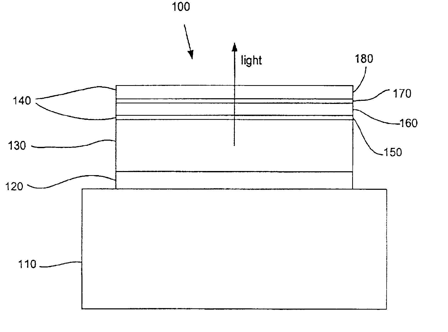
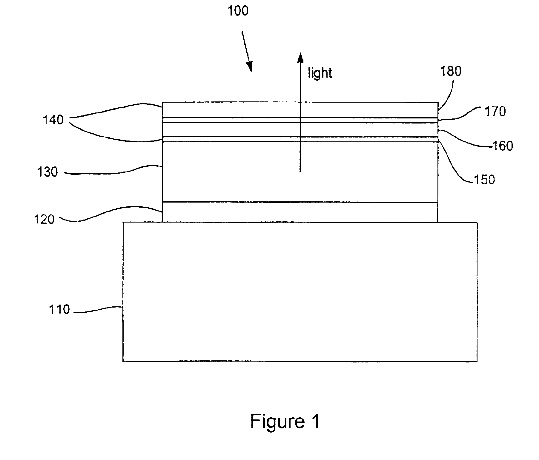
[0071]For comparative purposes, an array of OLEDs similar to the prior art was fabricated by depositing the following layers, in sequence, through appropriate masks. The deposition of all material was by thermal evaporation, except for ITO (which was only deposited in examples 2, 3 and 4), which was deposited by sputtering. Due to the use of different feedback mechanisms to monitor the deposition sources, the source parameter that was controlled may be either a temperature or a voltage. The MgAg layer was co-deposited from separate Mg and Ag targets to the total thickness shown (1000 Å in example 1).

[0072]

MaterialDep. Rate (Å / s)ThicknessSource Temperature (C.) or PowerCuPc1.2100345.1C.NPD3500254.4C.Alq3500266.7C.LiF1-21441.2VAl21088.9VCuPc2400387.4C.MgAg  3 (Mg)100040.5V1.2 (Ag)—43.5V

[0073]Although an Ag deposition rate of 1.2 was read on the dial, it is expected that the deposition rate was actually about 0.3 due to a tooling factor in this and in the other examples.

example 2

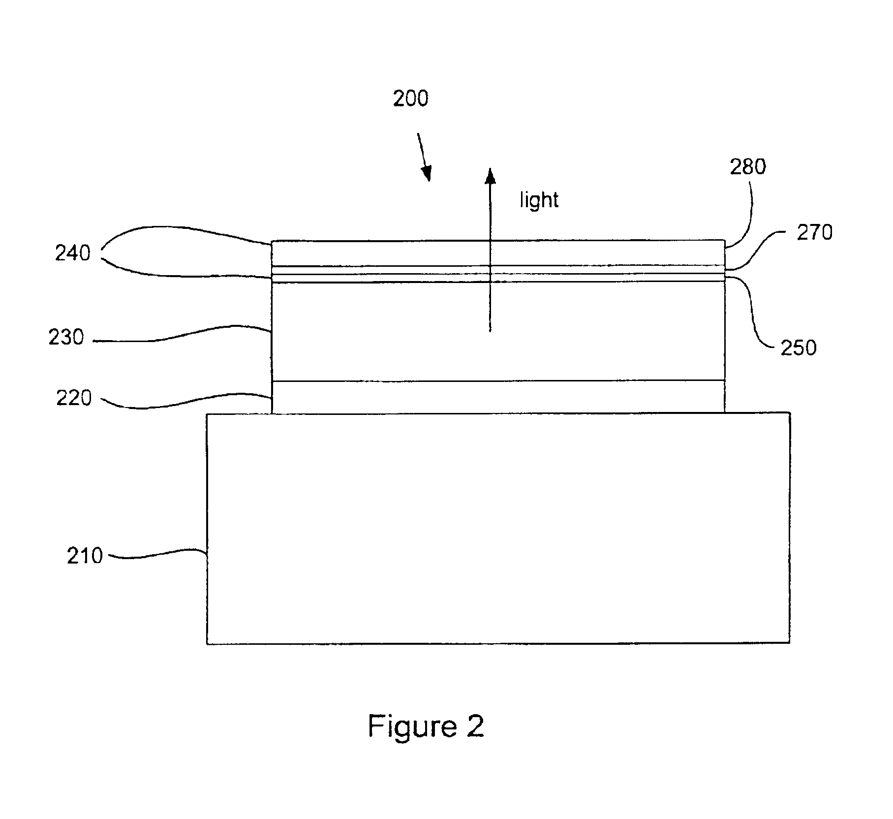
[0074]An array of OLEDs similar to the device shown in FIG. 1 was fabricated by depositing the following layers, in sequence. The equipment and masks used were the same as for example 1:

[0075]

MaterialDep. Rate (Å / s)ThicknessSource Temperature (C.) / PowerCuPc1.2100345.1C.NPD3500257-258C.Alq3500304-331C.LiF1-21440.9-41.4VAl21088.9VCuPc2400347-396C.MgAg  3 (Mg)10041.5V1.2 (Ag)—43.5V

[0076]A layer of ITO was then deposited by sputtering. The chamber contained 3 mTorr of an Ar / O2 mixture, and the power applied to the chamber was about 250 W. The power applied to the target was about 1.25-1.26 A at 1.98.6-197 V. The substrate was passed over the target 3 times at a speed of 17 inches per minute. With these parameters, it is expected that the thickness of ITO deposited was about 500 Å.

example 3

[0077]An array of OLEDs similar to the device shown in FIG. 3 was fabricated by depositing the following layers, in sequence. The equipment and masks used were the same as for example 1:

[0078]

MaterialDep. Rate (Å / s)ThicknessSource Temperature (C.) / PowerCuPc1.2100345.1C.NPD3500249C.Alq3500263C.LiF1-21440.0-40.7VAl21088.9VCuPc2400348C.

[0079]A layer of ITO about 500 Å thick was deposited by sputtering using parameters similar to those given for example 2, and the power applied to the target was 1.26 A at 198.3-197.5 V.


PUM


Abstract

A cathode adapted for use in an organic optoelectronic device is provided. The cathode has an electron injection layer, an organic buffer layer, a conducting layer, and a transparent conductive oxide layer disposed, in that order, over the organic operative layers of the optoelectronic device. A method of fabricating the cathode is also provided.

Description

[0001]The subject matter of this application is related to concurrently filed patent application Ser. No. 09 / 931,939, which is incorporated by reference in its entirety.RESEARCH AGREEMENTS[0002]The claimed invention was made by, on behalf of, and / or in connection with one or more of the following parties to joint university-corporation research agreement: Princeton University, The University of Southern California and Universal Display Corporation. The agreement was in effect on and before the date the claimed invention was made, and the claimed invention was made as a result of activities undertaken within the scope of the agreement.FIELD OF THE INVENTION[0003]The present invention relates to the field of organic semiconductor devices, and more particularly to transparent electrodes used in such devices.BACKGROUND OF THE INVENTION[0004]Opto-electronic devices that make use of organic materials are becoming increasingly desirable for a number of reasons. Many of the materials used t...

Claims


Application Information

Patent Timeline
IPC IPC(8): H05B33/00H01L51/52H05B33/14H05B33/26
CPCH01L51/0021H01L51/5221H05B33/14Y10S428/917H01L2251/5323H01L2251/5315H10K71/60H10K2102/3031H10K2102/3026H10K59/80524H10K50/828
Inventor LU, MIN-HAO MICHAELWEAVER, MICHAEL S.
Owner UNIVERSAL DISPLAY
Why Eureka
Try Eureka