Antenna and dielectric substrate for antenna

a dielectric substrate and antenna technology, applied in the direction of resonant antennas, antenna earthings, elongated active element feeds, etc., can solve the problems of poor vswr characteristic in a frequency range lower than f/sub>l and insufficient characteristics for use in dual-band antennas

Inactive Publication Date: 2006-07-04
TAIYO YUDEN KK
View PDF67 Cites 22 Cited by
  • Summary
  • Abstract
  • Description
  • Claims
  • Application Information

AI Technical Summary

Benefits of technology

[0020]By disposing the resonant element as stated above, the characteristics of the planar element and the reson...

Problems solved by technology

By the element 1014a, the antenna also resonates at a frequency lower than fL, and multi-resonance is realized, however, the VSWR characteristic in a frequency range lower than fL is poor, and sufficient chara...

Method used


Image

  • Antenna and dielectric substrate for antenna
  • Antenna and dielectric substrate for antenna
  • Antenna and dielectric substrate for antenna

Examples


first embodiment

1. First Embodiment

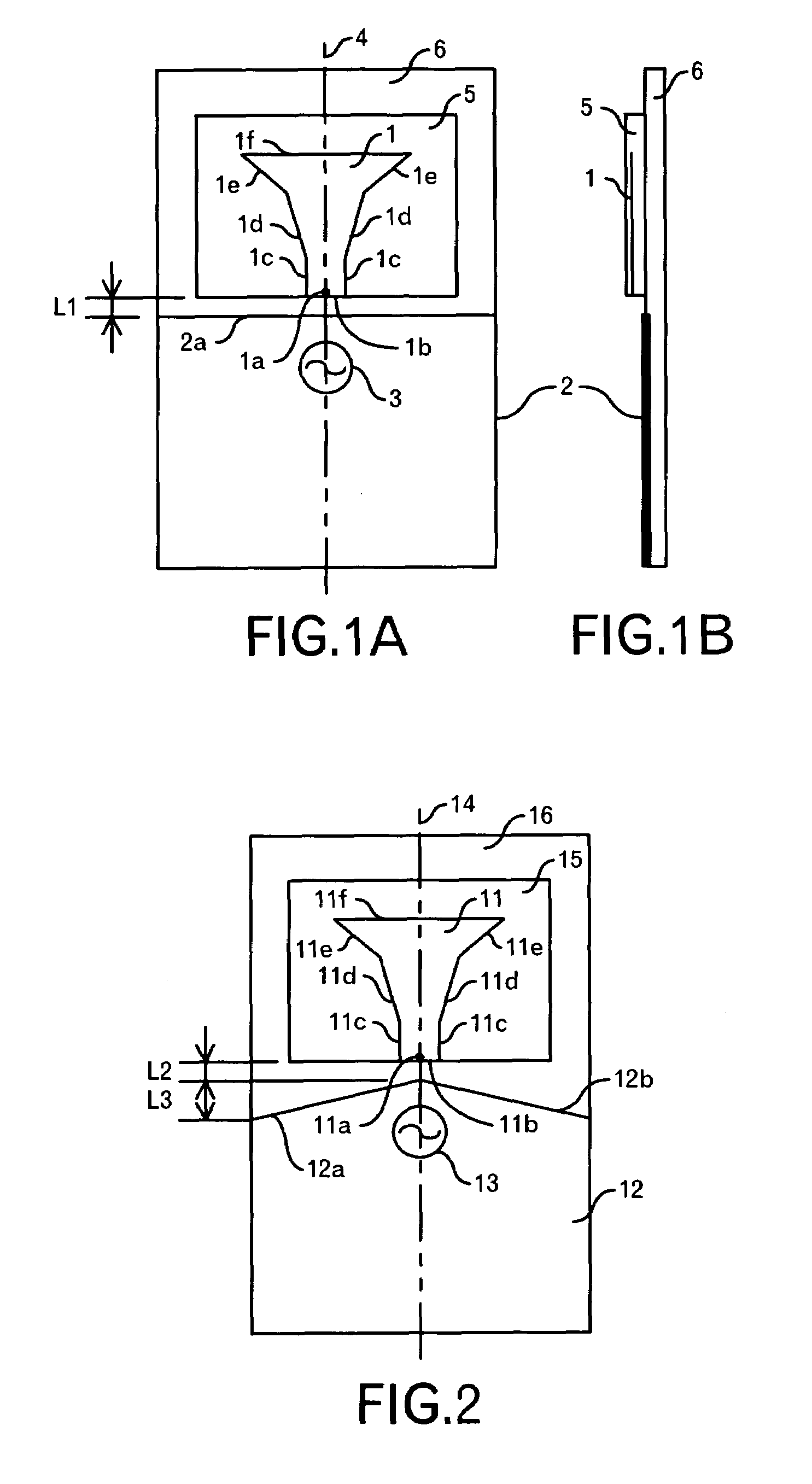
[0049]FIGS. 1A and 1B show the structure of an antenna of a first embodiment of this invention. As shown in FIG. 1A, the antenna of this embodiment is constituted by a dielectric substrate 5 including a planar element 1 in the inside thereof and having a dielectric constant of about 20, a ground pattern 2 juxtaposed with the dielectric substrate 5, a substrate 6, for example, a printed circuit board (more specifically, a resin substrate made of FR-4, Teflon (registered trademark) or the like), and a high frequency power source 3 connected to a feed point 1a of the planar element 1. The planar element 1 has a shape similar to a T shape, and is constituted by a bottom side 1b along an end portion of the dielectric substrate 5, sides 1c extending upward, sides 1d having a first inclination angle from the sides 1c, sides 1e having an inclination angle larger than the first inclination angle from the sides 1c, and a top portion 1f. The feed point 1a is provided at the ...

embodiment 2

2. Embodiment 2

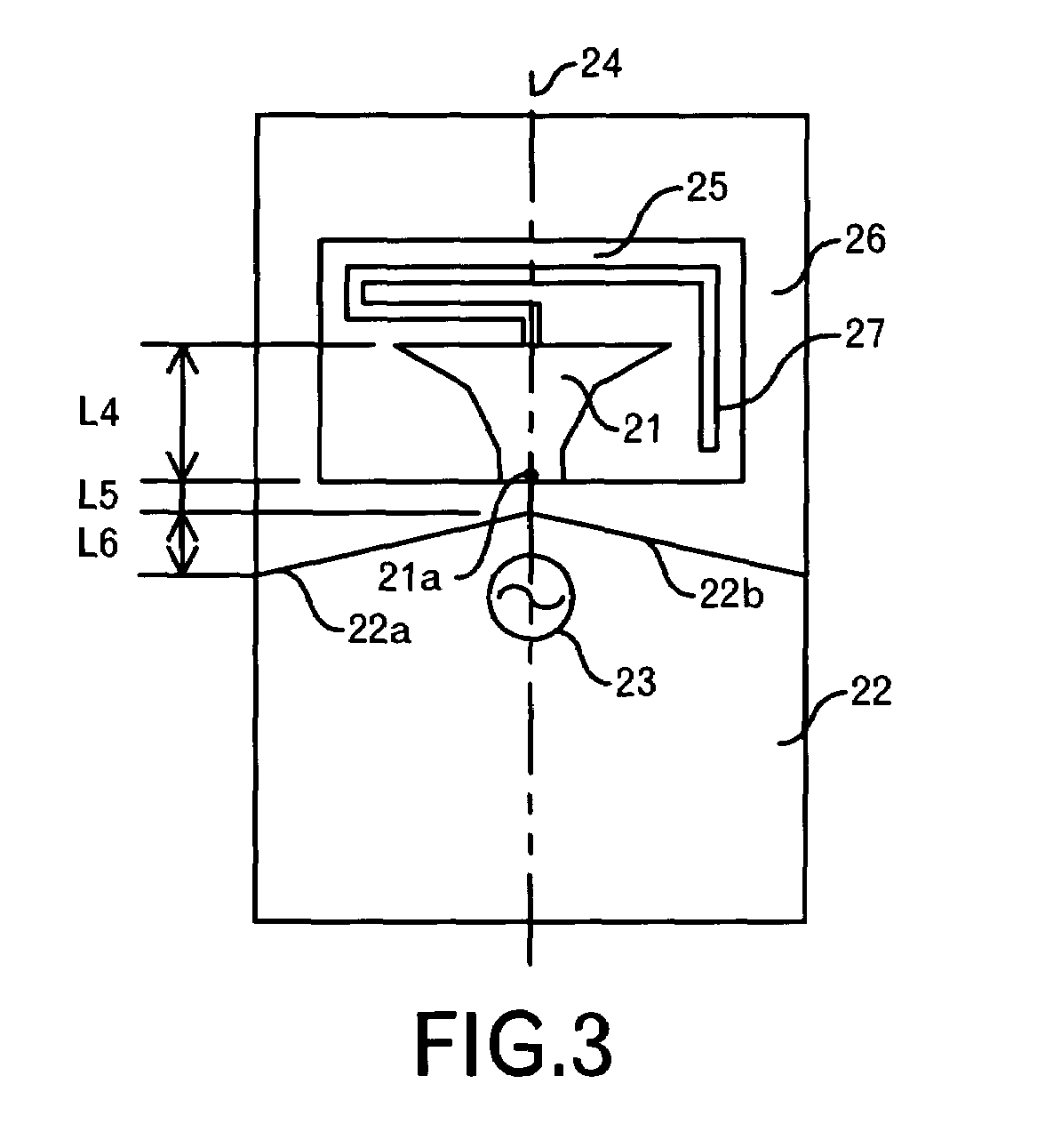
[0058]FIG. 2 shows a structure of an antenna of a second embodiment of this invention. As shown in FIG. 2, the antenna of this embodiment is constituted by a dielectric substrate 15 including a planar element 11 in the inside thereof and having a dielectric constant of about 20, a ground pattern 12 juxtaposed with the dielectric substrate 15, a substrate 16, for example, a printed circuit board, and a high frequency power source 13 connected to a feed point 11a of the planar element 11. The planar element 11 and the dielectric substrate 15 are the same as the planar element 1 and the dielectric substrate 5 of the first embodiment. In this embodiment, a distance L2 between the dielectric substrate 15 and the ground pattern 12 is 1.5 mm. Besides, the width of the ground pattern 12 is 20 mm.

[0059]Besides, the planar element 11 and the ground pattern 12 are symmetrical with respect to a straight line 14 passing through the feed point 11a. Besides, a length (hereinafter re...

embodiment 3

3. Embodiment 3

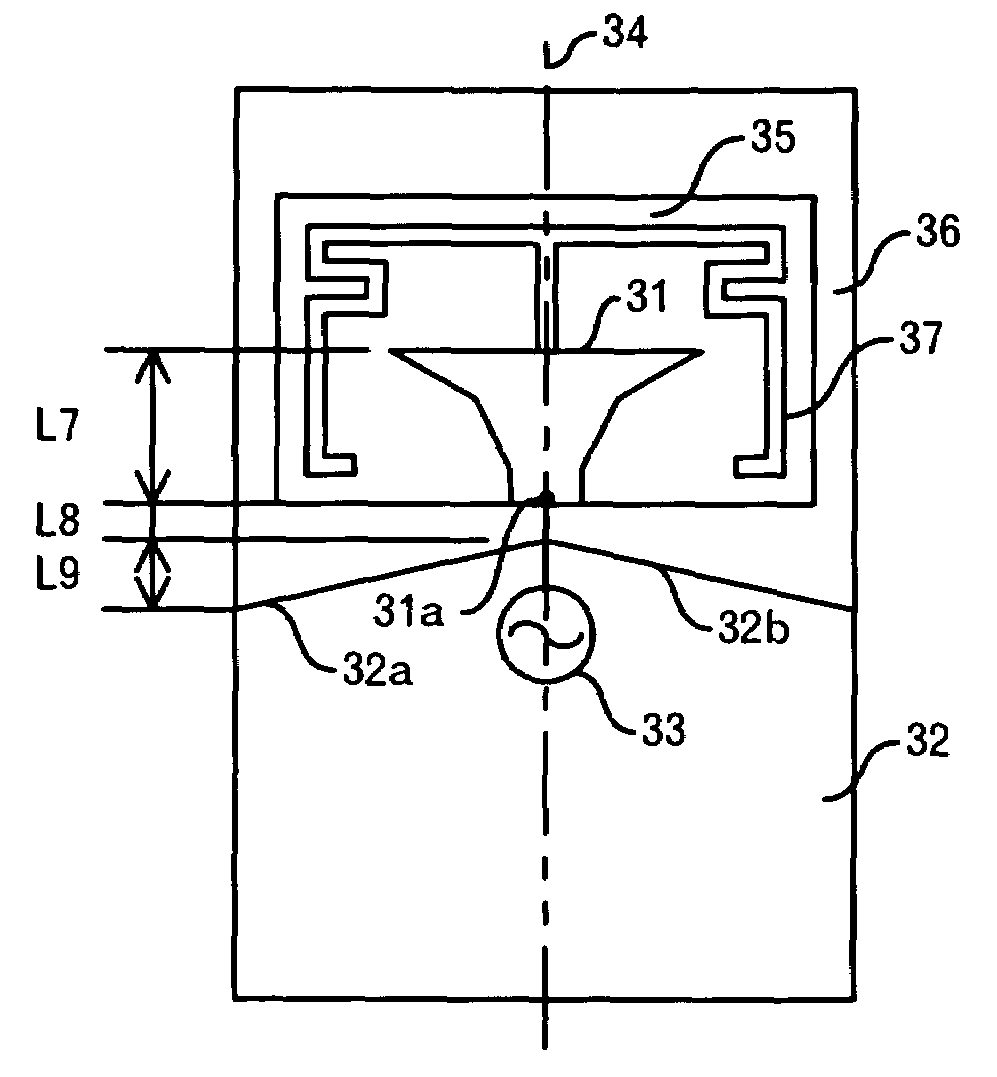
[0062]An antenna of a third embodiment of this invention is a dual band antenna for a 2.4 GHz band and a 5 GHz band. As shown in FIG. 3, the dual band antenna is constituted by a dielectric substrate 25 including in the inside thereof a planar first element 21 and a second element 27 as a resonant element extending from a center of a top of the first element 21, a ground pattern 22 juxtaposed with the dielectric substrate 25, disposed therefrom by an interval L5 (=1.5 mm) and having an upper edge portion of a tapered shape with respect to the dielectric substrate 25, a substrate 26 on which the dielectric substrate 25 and the ground pattern 22 are placed, and a high frequency power source 23 connected to a feed point 21a provided at the central portion of a bottom of the first element 21. The size of the dielectric substrate 25 is, for example, 8 mm×4.5 mm×1 mm. Incidentally, the ground pattern 22 may be formed inside the substrate 26.

[0063]The first element 21 has a ...


PUM


Abstract

This invention relates to a dual band antenna having a novel shape, which enables miniaturization and bandwidth widening. The antenna includes a dielectric substrate for an antenna including a layer of a planar element having a side edge portion constituted by either one of a curved line and line segments which are connected to each other while their inclinations are changed stepwise, and a substrate on which the dielectric substrate is placed and a ground pattern having a tapered shape with respect to the dielectric substrate is formed. The dielectric substrate and the ground pattern are juxtaposed, and a distance between the ground pattern and the side edge portion is continuously increased to become saturated as a point on the side edge portion moves away from a straight line passing through a feed position of the planar element. A resonant element is connected to the planar element at an end point of the planar element on the straight line passing through the feed position. By providing the resonant element, the dual band antenna can be realized. Besides, by the above structure, miniaturization of the antenna and bandwidth widening can be realized.

Description

TECHNICAL FIELD OF THE INVENTION[0001]The present invention relates to a wide bandwidth antenna, a dual band antenna and a dielectric substrate used for those antennas.BACKGROUND OF THE INVENTION[0002]For example, a monopole antenna as shown in FIG. 16A is disclosed in “B-77: BROADBAND CHARACTERISTICS OF SEMI-CIRCULAR ANTENNA COMBINED WITH LINEAR ELEMENT”, Taisuke Ihara, Makoto Kijima and Koichi Tsunekawa, pp77 General Convention of The Institute of Electronics, Information and Communication Engineers, 1996 (hereinafter referred to as “non-patent document 1”). In FIG. 16A, a semicircular element 1010 is erected vertically to a earth plate 1011, and the closest point of the arc of the element 1010 to the earth plate 1011 serves as a feed portion 1012. The non-patent document 1 discloses that a frequency fL at which the radius of the circle corresponds approximately to a quarter wavelength is the lower limit. Besides, it describes an example in which as shown in FIG. 16B, an element 1...

Claims


Application Information

Patent Timeline
IPC IPC(8): H01Q1/26H01Q13/08H01Q1/38H01Q5/10H01Q5/15H01Q5/364H01Q9/18H01Q9/28H01Q9/38H01Q9/40
CPCH01Q9/40H01Q1/38
Inventor OKADO, HIRONORI
Owner TAIYO YUDEN KK
Why Eureka
Try Eureka