Systems and methods for transmitting electromagnetic energy in a photonic device

Active Publication Date: 2006-07-04
RGT UNIV OF CALIFORNIA
View PDF14 Cites 37 Cited by
  • Summary
  • Abstract
  • Description
  • Claims
  • Application Information

AI Technical Summary

Benefits of technology

[0007]The present invention is directed to systems and methods that allow for the high efficiency transmission of an incident electromagnetic wave into or through a periodic multilayered photonic device with significantly reduced velocity of wave propagation. In one embodiment, the photonic device includes a body having a front surface and a plurality of periodic segments physically coupled together along a first direction normal to the surface. The device can be receptive to an electromagnetic wave having a first frequency and incident at a direction oblique to the first direction. Each segment can include a first anisotropic dielectric layer havin

Problems solved by technology

First, there is the possibility of omnidirectional reflection when the incident wave is totally reflected by the stack, regardless of the direction of incidence upon the stack.
Second, there is the possibility of negative refraction when a tangential component of the energy flux of the transmitted wave is antiparallel to that of the incident wave.
Third, there is the dramatic slowdown of the transmitted wave near a photonic band edge frequency when the normal component of the transmitted wave group velocity vanishes along with the respective component of the energy flux.
But at higher frequencies, the magnetic materials displaying the required properties become rare, costly and problematic.
In addition, all magnetic materials with sufficiently strong circular birefringence also display a very strong temporal dispersion, which may not be acceptable in a number of applications.

Method used


Image

  • Systems and methods for transmitting electromagnetic energy in a photonic device
  • Systems and methods for transmitting electromagnetic energy in a photonic device
  • Systems and methods for transmitting electromagnetic energy in a photonic device

Examples


Embodiment Construction

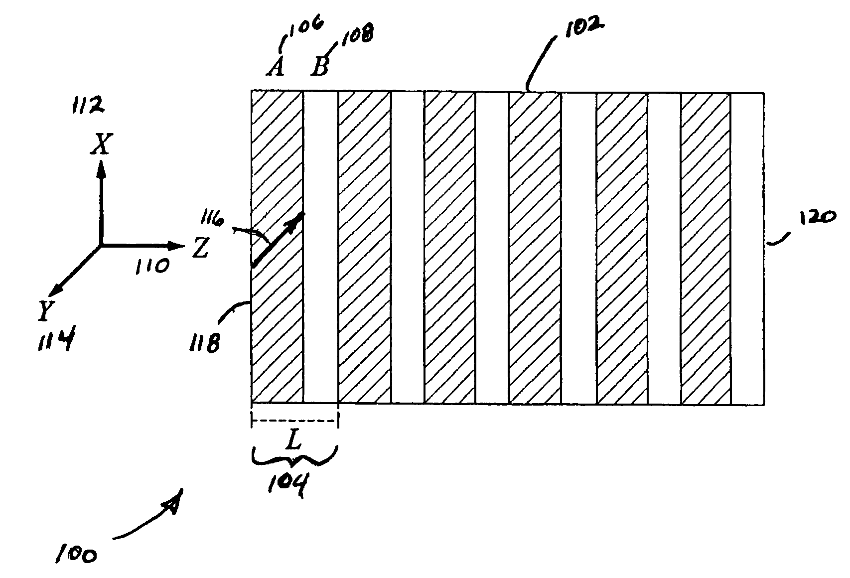
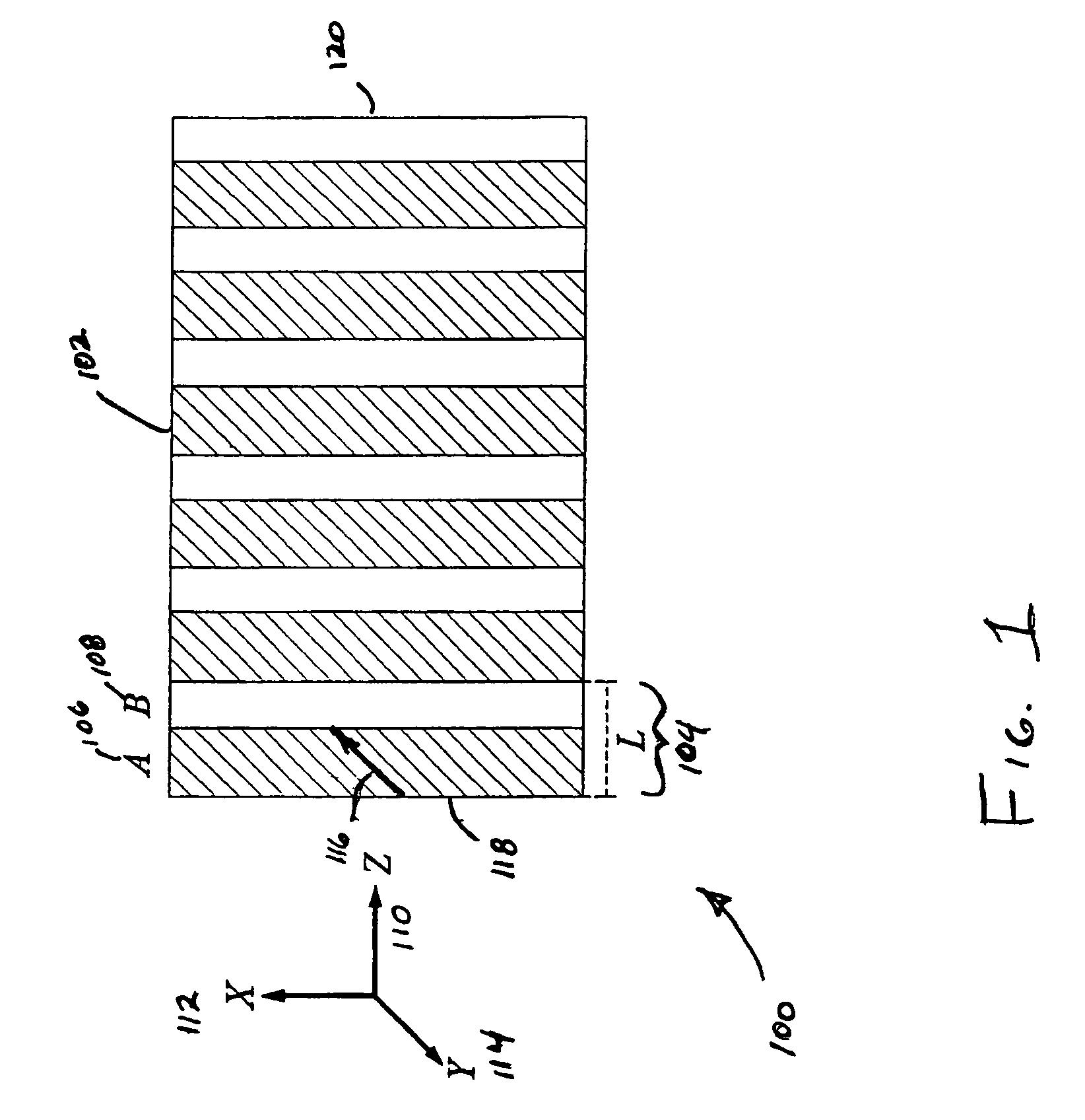
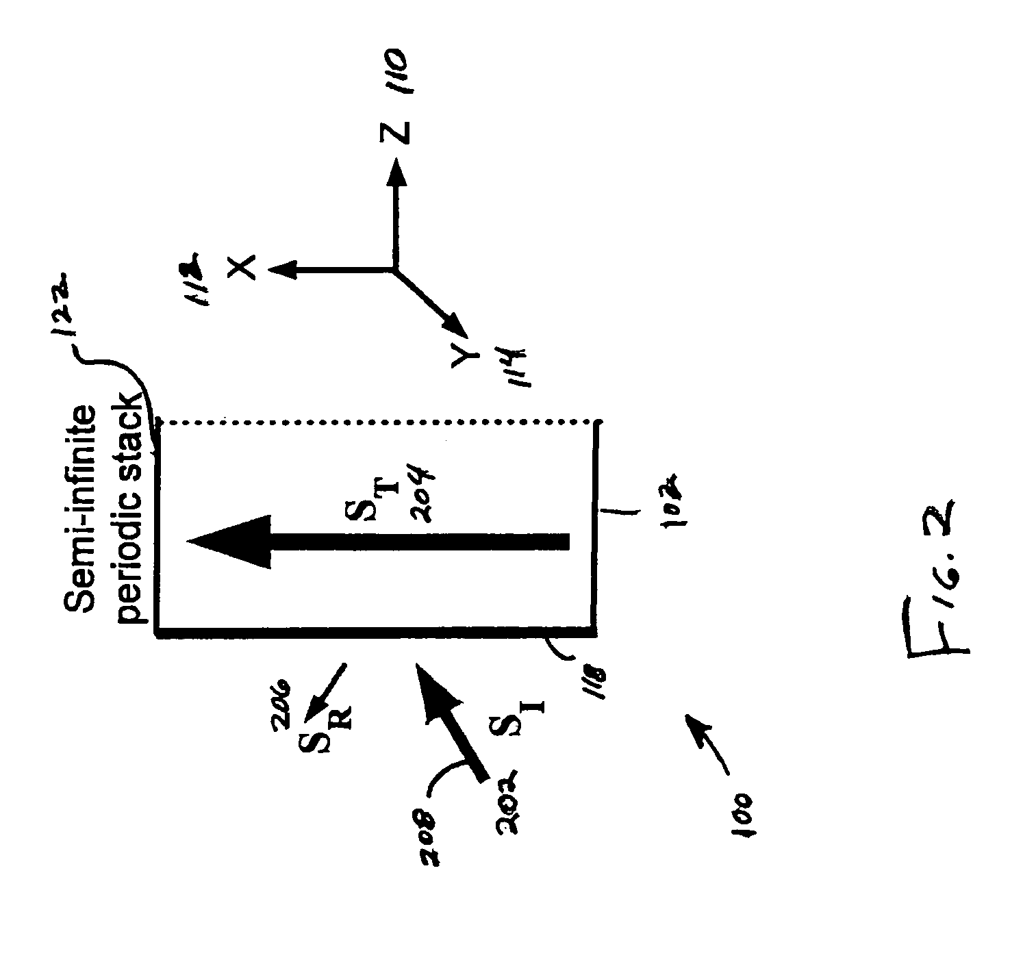
[0024]The systems and methods described herein provide for a photonic device capable of transmission of electromagnetic radiation with a greatly reduced group velocity at frequencies up to and including the ultraviolet range. More specifically, the photonic device is capable of electromagnetic transmission in at least two different reduced velocity modes, referred to herein as the axially frozen mode and the full frozen mode. The photonic device is preferably a periodic stack, or periodic layered array, of similar multi-layered segments. The photonic device can also have the geometry of a two or three dimensional photonic crystal. Preferably, at least one layer of each segment of the periodic stack is an anisotropic dielectric layer. In the axially frozen mode regime, a substantial portion of an electromagnetic wave, incident upon the surface of the photonic device, can be transmitted within the device and completely converted into a grazing mode with greatly reduced group velocity ...


PUM


Abstract

Systems and methods are provided that allow transmission of an electromagnetic wave in and through a periodic multilayered photonic device. The photonic device preferably is a periodic stack of plane-parallel layers with at least one them displaying dielectric anisotropy with a principle anisotropic axis forming an oblique angle with the normal to the layers. The wave obliquely incident on the surface of the device can be almost completely converted into an axially frozen mode characterized by a significantly increased amplitude, decreased group velocity normal to the incident surface and increased energy flux substantially tangential to the incident surface. The photonic device can be used in numerous applications over a wide range of frequencies up to and including the ultraviolet spectrum. The photonic device can be further configured with a deflection device which substantially increases the operational frequency range of the photonic device.

Description

CROSS-REFERENCE TO RELATED APPLICATIONS[0001]This application is based on U.S. provisional application Ser. No. 60 / 467,492, filed May 1, 2003, which is fully incorporated by reference herein.[0002]This invention was made with Government support under Contract No. F49620-01-1-0567, awarded by Air Force Office of Scientific Research. The Government has certain rights to this invention.FIELD OF THE INVENTION[0003]The invention relates generally to the field of photonic devices, and more particularly to systems and methods for transmitting an electromagnetic wave in a photonic device.BACKGROUND INFORMATION[0004]Electromagnetic properties of photonic devices, such as photonic crystals, have been a subject of research for decades. Of particular interest have been periodic stacks of dielectric layers. These stacked devices are typically composed of multiple repeating segments each having two or more dielectric layers with varying refractive indices. The segments are arranged in periodic ma...

Claims


Application Information

Patent Timeline
IPC IPC(8): G02B6/10
CPCG02B6/1225B82Y20/00
Inventor FIGOTIN, ALEKSANDRVITEBSKIY, ILYA
Owner RGT UNIV OF CALIFORNIA
Why Eureka
Try Eureka