Two-dimensional radiation detector

a detector and two-dimensional technology, applied in the direction of x/gamma/cosmic radiation measurement, instruments, radioation controlled devices, etc., can solve the problems of significant influence of noise component overlap on charge information converted from radiation, type of conventional technology, etc., to suppress the influence of noise emitted, no fluctuations in detection sensitivity

Active Publication Date: 2006-07-11
SHIMADZU CORP
View PDF7 Cites 4 Cited by
  • Summary
  • Abstract
  • Description
  • Claims
  • Application Information

AI Technical Summary

Benefits of technology

[0014]The present invention is developed by taking such problems into consideration. The object of the present invention is to provide a radiation detector that has no fluctuations in detection sensitivity and can suppress the influence of the noise emitted from the light source.
[0018]The noise emitted from light emitting means to the active matrix substrate or the semiconductor layer is blocked by the electromagnetic shield. Thus the overlapping of the charge information converted from the radiation information with the noise component can be prevented.
[0019]Consequently the radiation can be detected, without fluctuations of the detection sensitivity to radiation, by suppressing the influence of the noise emitted from light emitting means.
[0021]With the above implementation of the invention, the electromagnetic shield covers light emitting means so that it is not exposed but a light passage is secured for light emitting means to apply the light to the end face of the flat light guide. Thus the noise, which is emitted from light emitting means in directions other than the active matrix substrate or the semiconductor layer, is also shielded. Therefore, the influence of the noise to the semiconductor layer and the active matrix substrate can be suppressed more efficiently. Furthermore, the influence of the noise on the surrounding circuits of the radiation detector can be similarly suppressed.
[0023]With the above implementation of the invention, the noise emission from the power supply unit to the surrounding area can be prevented by including the grounded conductive layer in the power supply unit. Thus, the power supply unit can supply electric power to light emitting means without having noise influence the semiconductor layer, the matrix substrate and the charge information process unit. Furthermore, the charge information process unit can be disposed freely without taking the arrangement of the power supply unit into consideration.
[0024]With the radiation detector of the present invention, the light emitted from the light emitting unit can be applied to the semiconductor layer, while the noise from light emitting means is blocked. Furthermore, the radiation can be detected accurately without fluctuations in detection sensitivity because the radiation is detected under a condition that the light is applied to the semiconductor layer.

Problems solved by technology

However, this type of conventional technology has the following problems.
However, any kind of light source selected requires a power supply and an ordinary switching type power supply is suitable for this purpose because the switching type power supply is small, light weight and high capacity.
Since the charge information converted from radiation itself is weak, the influence of the noise component overlapping on the charge information converted from the radiation is significant.

Method used


Image

  • Two-dimensional radiation detector
  • Two-dimensional radiation detector
  • Two-dimensional radiation detector

Examples


first embodiment

[0032]The first embodiment of the present invention will be described, with reference to the drawings.

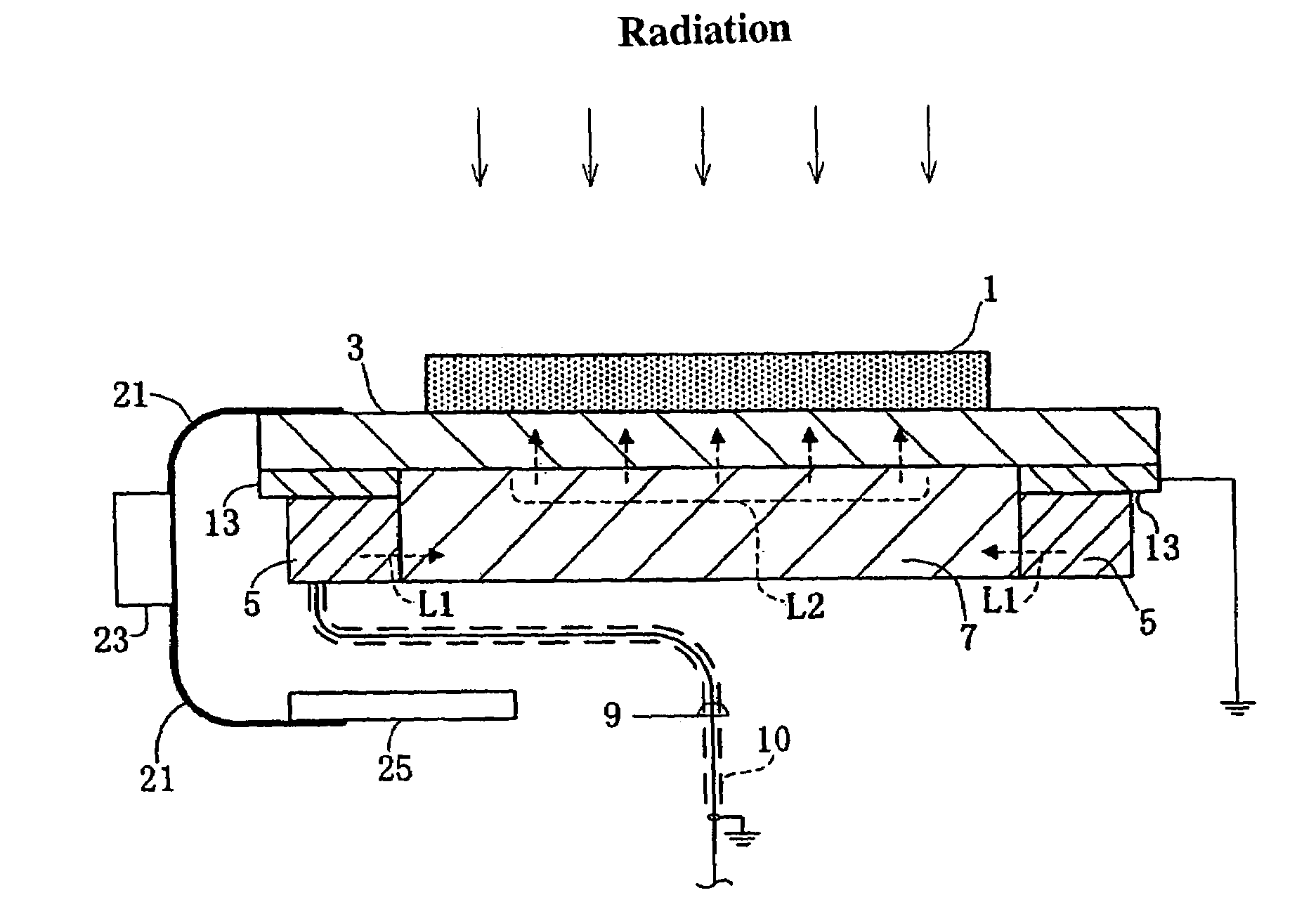
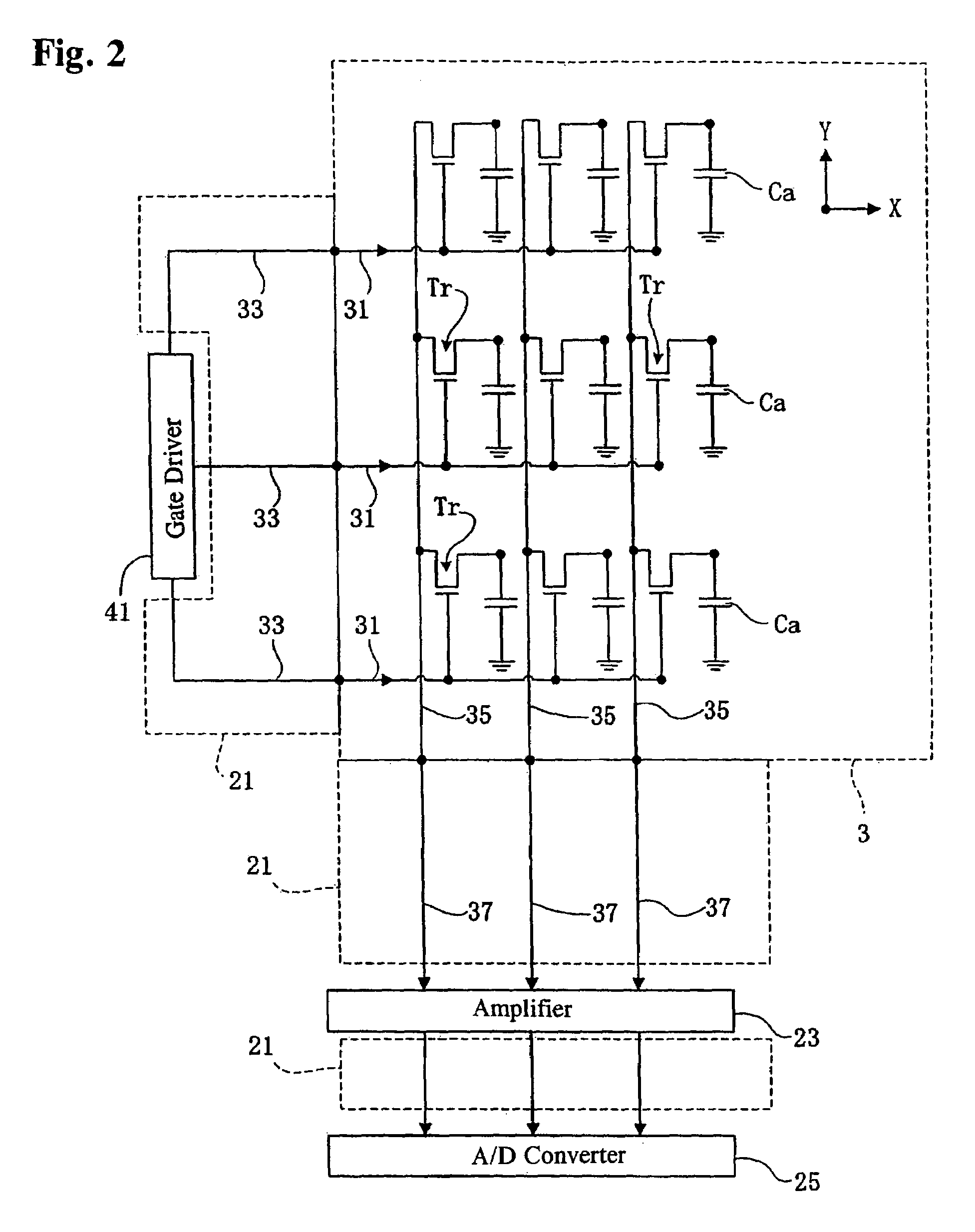
[0033]FIG. 1 is a cross-section showing the structure of a radiation detector according to a first embodiment and FIG. 2 is a simplified circuit diagram of an active matrix substrate, an amplifier and the like and a gate driver.

[0034]The radiation detector according to the first embodiment detects incident radiation to the direction of the solid line arrow as shown in FIG. 1. Radiation is, for example, X-ray and the like. The radiation detector is equipped with a radiation sensitive semiconductor thick film 1 and an active matrix substrate 3 that read out the charge information from the semiconductor thick film 1, wherein the semiconductor thick film 1 is formed on the surface of the active matrix substrate 3. A flat light guide 7 is disposed in the back side of the active matrix substrate 3 with the light emitting face of the flat light guide 7 directed to the active matrix substra...

second embodiment

[0060]Next, the second embodiment of the present invention will be explained. When the composition is the same as the first embodiment, detailed explanations are omitted and the same marks are used.

[0061]FIG. 3 is a simplified drawing showing the structure of a radiation detector according to a second embodiment.

[0062]The radiation detector according to the second embodiment contains an electromagnetic shield 13 that surrounds the light emitting unit 5. An opening is disposed on the electromagnetic shield 13 so that the light emitting unit 5 is allowed to emit light to an end face of the flat light guide 7. Thus, the electromagnetic shield 13, the vertical cross-section of which is shaped like a rectangle without one side, surrounds the light emitting unit 5. The opening, through which the light emitting unit 5 can illuminate, is located at the surface facing the flat light guide 7. Of course the electromagnetic shield 13 of the second embodiment is also made from a conductive mater...


PUM


Abstract

A radiation detector is provided that has no fluctuations in detection sensitivity and is capable of suppressing the influence of the noise emitted from a light source. In the radiation detector in the present invention, a light emitting unit applies light to the end face of a flat light guide. On receiving the light, the flat light guide emits flat light from its surface toward an active matrix substrate. The light is led to a semiconductor thick film after passing through the active matrix substrate. The noise emitted from the light emitting unit to the active matrix substrate or the semiconductor thick film can be blocked by an electromagnetic shield. An incident radiation to the semiconductor thick film in this condition can be detected while the effect of the noise emitted from the light emitting unit is suppressed, and fluctuations in radiation sensitivity do not occur.

Description

INCORPORATION BY REFERENCE[0001]The present application claims priority under 35 U.S.C. §119 to Japanese Patent Application No. 2004-122806 filed on Apr. 19, 2004. The content of the application is incorporated herein by reference in its entirety.BACKGROUND OF THE INVENTION[0002]The present invention relates to a two-dimensional radiation detector for use in medical, industrial as well as atomic power fields and the like to detect radiation.[0003]In the conventional art, the radiation detector of this type contains a radiation sensitive radiation converting layer (semiconductor layer) that converts radiation information into electric charge information and an active matrix substrate that reads out the converted electric charge.[0004]In the conventional radiation detector, the electric charge information obtained at the radiation converting layer is read out by the active matrix substrate, wherein the electric charge information is processed by an amplifier and the like, and output e...

Claims


Application Information

Patent Timeline
Patent Type & Authority Patents(United States)
IPC IPC(8): G01T1/24G01T1/29H01L27/14H01L27/146H01L31/09
CPCG01T1/2928H01L27/14676H01L27/14623H01L27/14609
Inventor WATANABE, NARUMIYOSHIMUTA, TOSHINORI
Owner SHIMADZU CORP
Why Eureka
Try Eureka