Connector to be fixed to a device and method of fixing a connector to a device

a technology of connecting wires and devices, applied in the direction of coupling device connections, electrical equipment, substation/switching arrangement details, etc., can solve the problems of unsuitable for situations and uncertain mechanical strength of construction, and achieve the effects of enhancing holding force, enhancing soldering area, and enhancing holding for

Active Publication Date: 2006-07-18
SUMITOMO WIRING SYST LTD
View PDF14 Cites 11 Cited by
  • Summary
  • Abstract
  • Description
  • Claims
  • Application Information

AI Technical Summary

Benefits of technology

[0009]Solder enters the solder entering recess to increase the soldering area and to enhance a holding force on the electric / electronic device. Solder that enters the solder entering recess is locked by the lock on the peripheral edge of the solder entering recess to enhance the holding force. As a result, fixing reliability to the electric / electronic device is improved.
[0010]The solder entering recess preferably is substantially elliptical. Thus, the soldering area can be increased further as compared to a right circular solder entering recess. Further, burrs are less likely to be formed on the peripheral edge of the solder entering recess as compared to a rectangular solder entering recess.

Problems solved by technology

The outwardly bulging board fixing portions require a large space on the circuit board.
Thus, the above-described connector is not well suited for situations where space must be saved.
However, this construction has uncertain mechanical strength as compared to the screw-fastening construction.

Method used


Image

  • Connector to be fixed to a device and method of fixing a connector to a device
  • Connector to be fixed to a device and method of fixing a connector to a device
  • Connector to be fixed to a device and method of fixing a connector to a device

Examples


Embodiment Construction

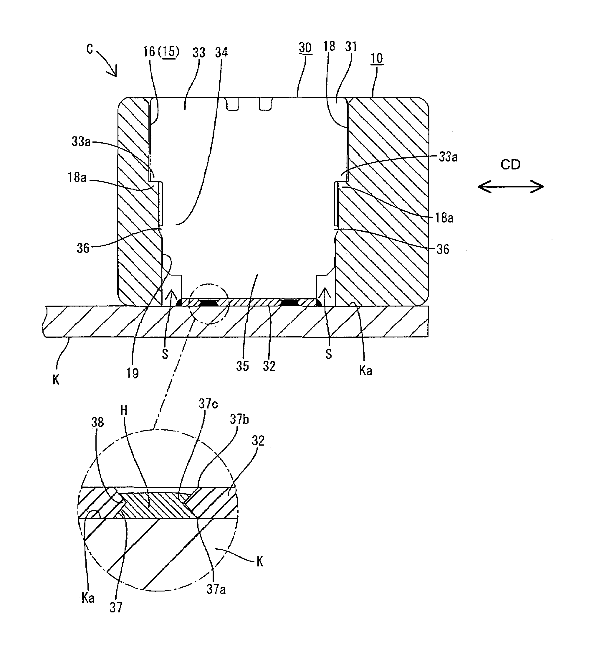
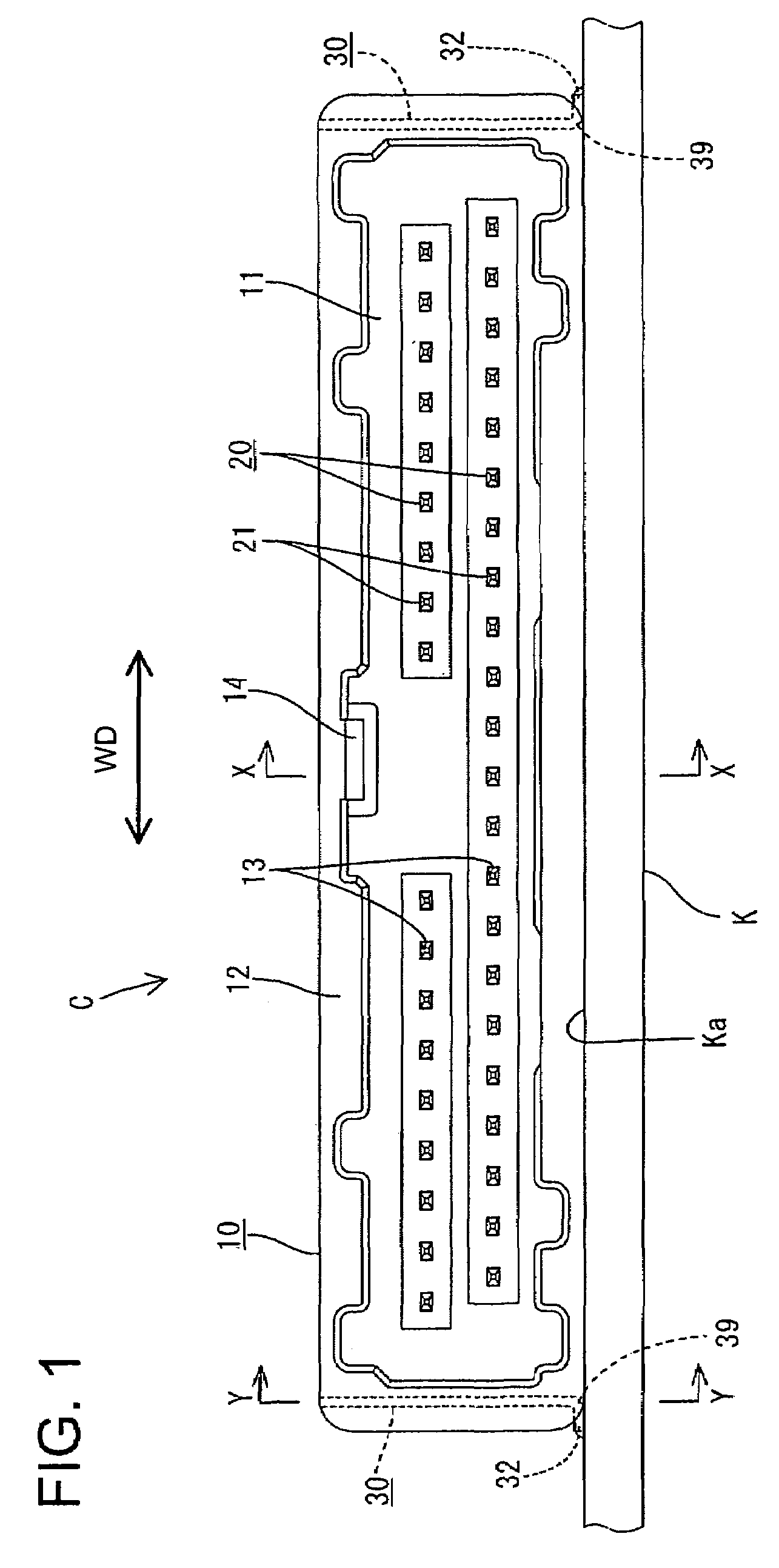
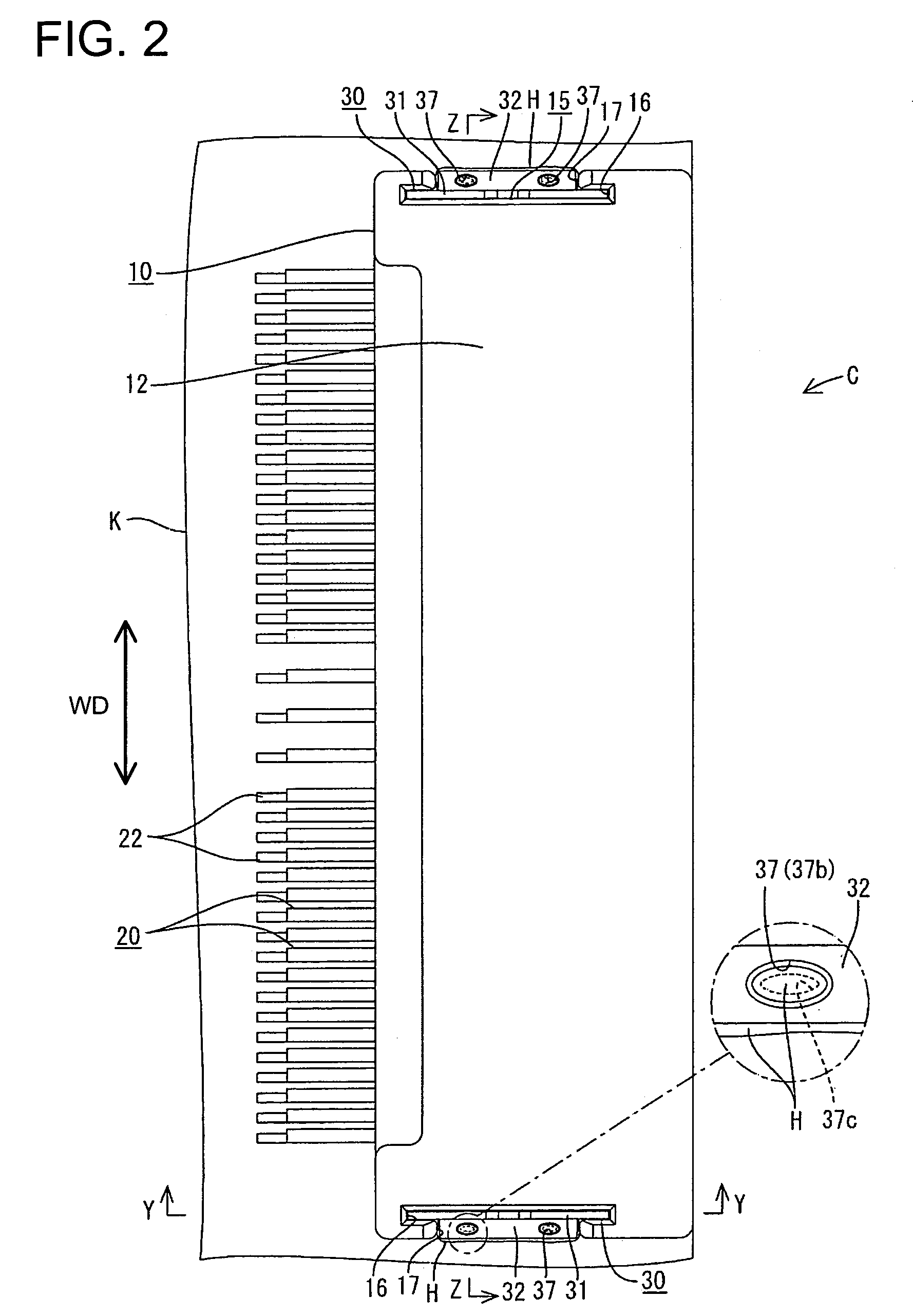
[0025]A circuit board connector according to the invention is identified by the letter C in FIGS. 1 to 6 and is to be connected with a circuit board K or other electric or electronic device, such as a junction box, dash panel, etc. The connector C includes a housing 10 and terminal fittings 20 are mounted in the housing 10. Fixing members 30 are mountable into the housing 10 for fixing the housing 10 to the circuit board K. In the following description, a side (right side in FIG. 3) of the housing 10 to be connected with the mating housing is referred to as the front, and reference is made to all the figures except FIG. 2 concerning the vertical direction.

[0026]The housing 10 is wide and includes a terminal holding portion 11 for holding the terminal fittings 20. A receptacle 12 projects forward from a front peripheral edge of the terminal holding portion 11. The terminal holding portion 11 is formed with terminal insertion cavities 13 and the terminal fittings 20 are insertable the...


PUM


Abstract

Fixing members (30) fixable to a circuit board (K) by soldering are mounted in a housing (10). Each fixing member (30) is comprised of a main panel (31) and a solder leg (32) projecting sideways from the bottom end of the main portion (31). The solder leg (32) has solder entering holes (37) that open at a side of the solder leg (32) toward the circuit board K and at a side opposite therefrom. Each solder entering hole (37) has a cross-section that gradually increases toward both upper and lower open ends (37a, 37b). A locking portion (38) is formed on each solder entering hole (37) and bulges more inward than both open ends (37a, 37b). The locking portion (38) locks solder (H) that enters the solder entering hole (37).

Description

BACKGROUND OF THE INVENTION[0001]1. Field of the Invention[0002]The invention relates to a connector to be mounted to an electric or electronic device, in particular to a circuit board connector, and to a method of mounting or fixing a connector to an electric or electronic device.[0003]2. Description of the Related Art[0004]Japanese Unexamined Patent Publication No. H06-203896 discloses a circuit board connector that has a housing with opposite side surfaces. Board fixing portions are formed integrally with the housing and bulge out sideways from the bottom ends of the opposite side surfaces. The board fixing portions are formed with internally threaded holes. Screws are inserted through screw insertion holes of the circuit board and are fastened to the internally threaded holes.[0005]The outwardly bulging board fixing portions require a large space on the circuit board. Thus, the above-described connector is not well suited for situations where space must be saved.[0006]A circuit ...

Claims


Application Information

Patent Timeline
Patent Type & Authority Patents(United States)
IPC IPC(8): H01R13/60H01R13/73
CPCH01R12/707H01R12/57
Inventor NAKANO, HIROSHIOKAMURA, KENJI
Owner SUMITOMO WIRING SYST LTD
Why Eureka
Try Eureka