Circuit having source follower and semiconductor device having the circuit

a source follower and circuit technology, applied in the field of source follower, can solve the problems of hardly secure enough time for correction, inability to employ methods in the circuit, and large circuit scal

Inactive Publication Date: 2006-07-25
SEMICON ENERGY LAB CO LTD
View PDF14 Cites 5 Cited by
  • Summary
  • Abstract
  • Description
  • Claims
  • Application Information

AI Technical Summary

Benefits of technology

[0021]According to the above configuration of the invention, an output potential of the source follower is prevented from varying due to an influence of a change in potential of the power supply line connected to the source follower. This method is quite simple since it requires no additional signal lines unlike the case of using a correction circuit. In addition, since time for correction is not required unlike the case of using a correction circuit, the invention can be applied to such a circuit as to output signals constantly.

Problems solved by technology

In addition, this method cannot be employed in the circuit which can hardly secure enough time for correction.
However, these methods are disadvantageous in that the circuit scale becomes quite large.

Method used


Image

  • Circuit having source follower and semiconductor device having the circuit
  • Circuit having source follower and semiconductor device having the circuit
  • Circuit having source follower and semiconductor device having the circuit

Examples


embodiment mode 1

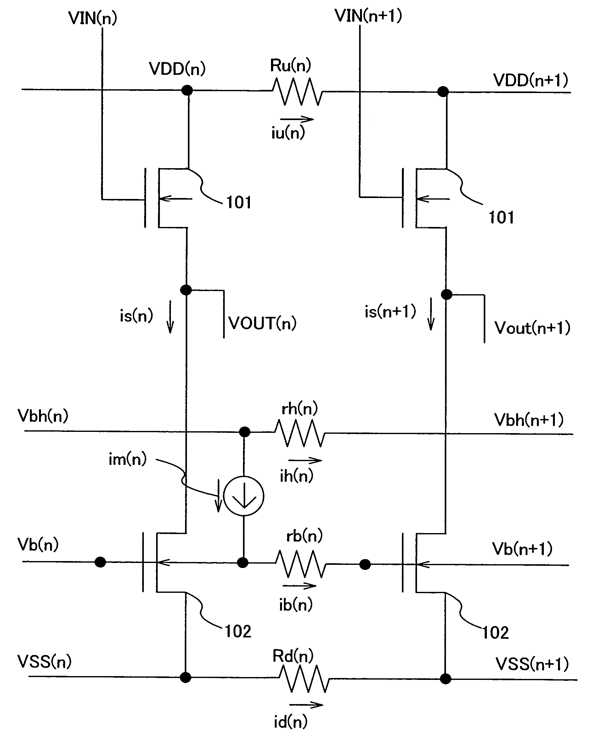
[0030]FIG. 1 is a circuit diagram as one mode of the circuit having source followers of the invention.

[0031]A power supply line Vbh is provided and an appropriate constant current source is disposed between power supply lines Vbh and Vb. The constant current source may be a resistor. By efficiently setting a current value flowing in the constant current source, the potential change of the power supply line Vb is adjusted to be equal to the potential change of the power supply line VSS.

[0032]FIG. 1 includes two source followers each including N-channel transistors 101 and 102.

[0033]As shown in FIG. 1, a current flowing in an n-th source follower is denoted by is(n), a potential of the high potential power supply line is denoted by VDD(n), a potential of the low potential power supply line is denoted by VSS(n), a potential of the power supply line for specifying a value of the constant current is denoted by Vb(n) and a potential of a power supply line which is additionally provided ac...

embodiment mode 2

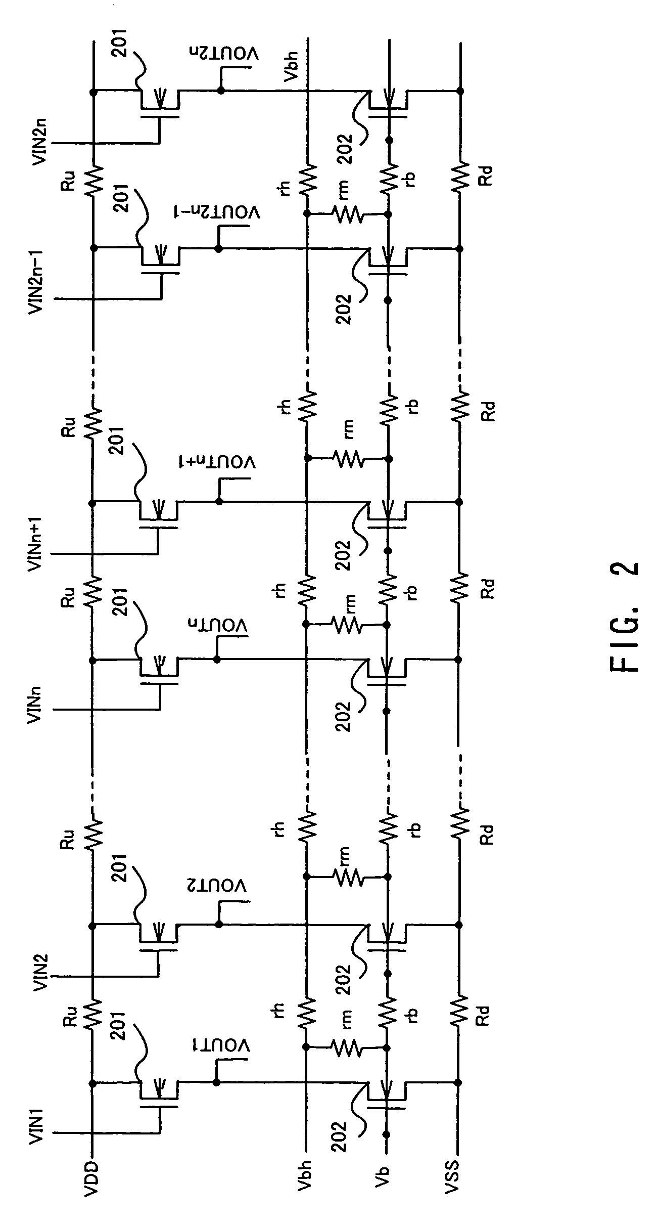
[0042]FIG. 2 includes 2n source followers each including N-channel transistors 201 and 202. Power supply lines are connected to each of right and left ends of the source followers.

[0043]It is assumed here that all the transistors have the same size, and a power supply line connecting each source follower or the like has the same resistance value among all the source followers.

[0044]As shown in FIG. 2, the high potential power supply line is denoted by VDD, the low potential power supply line is denoted by VSS, a power supply line for specifying a value of a constant current is denoted by Vb, a power line newly added for the present invention id denoted by Vbh, a resistor in the VDD between each source follower is denoted by Ru, a resistor in the VSS between each source follower is denoted by Rd, a resistor in the Vb is denoted by rb, a resistor in the Vbh is denoted by rh and a resistor disposed between the Vb and Vbh in each source follower is denoted by rm. Although rm is desirabl...

embodiment 1

[0058]Described in this embodiment is a configuration of a semiconductor device using the driver circuit having source followers of the invention shown in FIG. 2. FIG. 4 is a block diagram of a semiconductor device of this embodiment. The semiconductor device shown in FIG. 4 includes a pixel portion 411 having pixels each having a display element, a scan line driver circuit 412 for selecting each pixel, and a signal line driver circuit 413 for controlling the input of a video signal to the selected pixel. By using the circuit having source followers of the invention in the signal line driver circuit 413 of the semiconductor device in FIG. 4, variations of the source followers can be suppressed, and thus luminance unevenness is prevented from being recognized in the display portion 411.

[0059]The signal line driver circuit 413 in FIG. 4 includes a shift register 414, an analog latch A 415, an analog latch B 416 and source followers 417.

[0060]The shift register 414 is input with clock ...


PUM


Abstract

When a potential of a power supply line varies according to a flowing current, the gate-source voltage Vgs of a transistor also varies, leading to variations in the constant current between each source follower. In order to solve this problem, a potential Vb of the gate terminal of a transistor as a constant current source is changed in the same manner as a power supply line Vss which is connected to the source terminal of the transistor. Therefore, variations in the constant current are suppressed and variations in the output of the source followers are thus suppressed. In addition, by connecting the circuit having source followers to the output side of a signal line driver circuit, it can be prevented that luminance unevenness of a striped pattern is recognized in a display portion of a semiconductor device.

Description

BACKGROUND OF THE INVENTION[0001]1. Field of the Invention[0002]The present invention relates to a source follower, and more particularly to a semiconductor device having amplifiers such as source followers formed by using thin film transistors in a driver circuit.[0003]It should be noted that a semiconductor device in this specification refers to all the devices which function by the use of semiconductor characteristics. For example, an electro-optical apparatus, a semiconductor circuit, and an electronic apparatus all fall in the category of the semiconductor device.[0004]2. Description of the Related Art[0005]FIG. 7 is a circuit diagram of a general source follower. In the source follower shown in FIG. 7, an input potential Vin is supplied to the gate (G) of a transistor 901 while a potential Vdd (Vdd>Gnd (ground potential)) is supplied to the drain (D) thereof. In addition, the source (S) of the transistor 901 is connected to a constant current source 902 and a potential of t...

Claims


Application Information

Patent Timeline
Patent Type & Authority Patents(United States)
IPC IPC(8): H03K19/0175G11C11/14G11C11/44H03K19/082H03K19/094G09G3/20G09G5/00H03F1/30H03F3/50H03K19/00
CPCG09G3/20H03F3/505H03F1/301G09G2310/0275
Inventor MIYAKE, HIROYUKISHIONOIRI, YUTAKA
Owner SEMICON ENERGY LAB CO LTD
Why Eureka
Try Eureka