Lattice strain measuring system and method

a strain measuring system and strain technology, applied in the direction of material analysis using wave/particle radiation, instruments, nuclear engineering, etc., can solve the problems of coarse spatial resolution power, inability to evaluate micronized electronic devices, and methods whose spatial resolution power is coarse, etc., to achieve high resolution power, short period of time, and high accuracy

Active Publication Date: 2006-08-01
FUJITSU LTD
View PDF6 Cites 7 Cited by
  • Summary
  • Abstract
  • Description
  • Claims
  • Application Information

AI Technical Summary

Benefits of technology

[0020]An object of the present invention is to provide a lattice strain measuring system and method, and a stress measuring system and method which can understandably display lattice strain magnitudes, etc. with high resolving power and with high accuracy.
[0029]According to the present invention, a scanning transmission electron microscope is used, whereby electron beams are caused to scan to thereby suitably set an incidence position. Accordingly, the incidence position of the electron beams can be displaced at a nanometer-order pitch accurately in a short period of time. The use of a scanning transmission electron microscope requires no image forming lens below a sample, and the convergent-beam electron diffraction image is free from the distortion due to the influence of an image forming lens. Thus, according to the present invention, a distribution of lattice strains in an electronic device having, e.g., a micronized structure of nanometer order can be displayed in an image with high resolving power and with high accuracy and furthermore in a short period of time.
[0030]According to the present invention, a scanning transmission electron microscope is used, whereby data of electron microscope images associated with coordinates of respective measurement positions can be obtained. The data of electron microscope images and the data of lattice strain magnitudes are both associated with the same coordinate system, which enables an electron microscope image and the image of a lattice strain distribution can be displayed, associated with each other. According to the present invention, the image of a lattice strain distribution and an electron microscope image can be understandably displayed, associated with each other, which permits the measured results to be readily used as a useful guide for the device development.
[0032]According to the present invention, stresses in respective points of a sample are computed, based on lattice strain magnitudes given by the lattice strain measuring system and method described above, whereby distributions of stresses generated in an electronic device of a micronized structure can be displayed in images with high resolving power and high accuracy and furthermore in a short period time. Furthermore, a stress distribution image can be understandably displayed, associated with an electron microscope image, which makes it possible to use the measured results to be used as a useful guide in the device development.

Problems solved by technology

However, these methods, whose spatial resolving power is coarse, can not be used to evaluate micronized electronic devices.

Method used


Image

  • Lattice strain measuring system and method
  • Lattice strain measuring system and method
  • Lattice strain measuring system and method

Examples


first embodiment

A First Embodiment

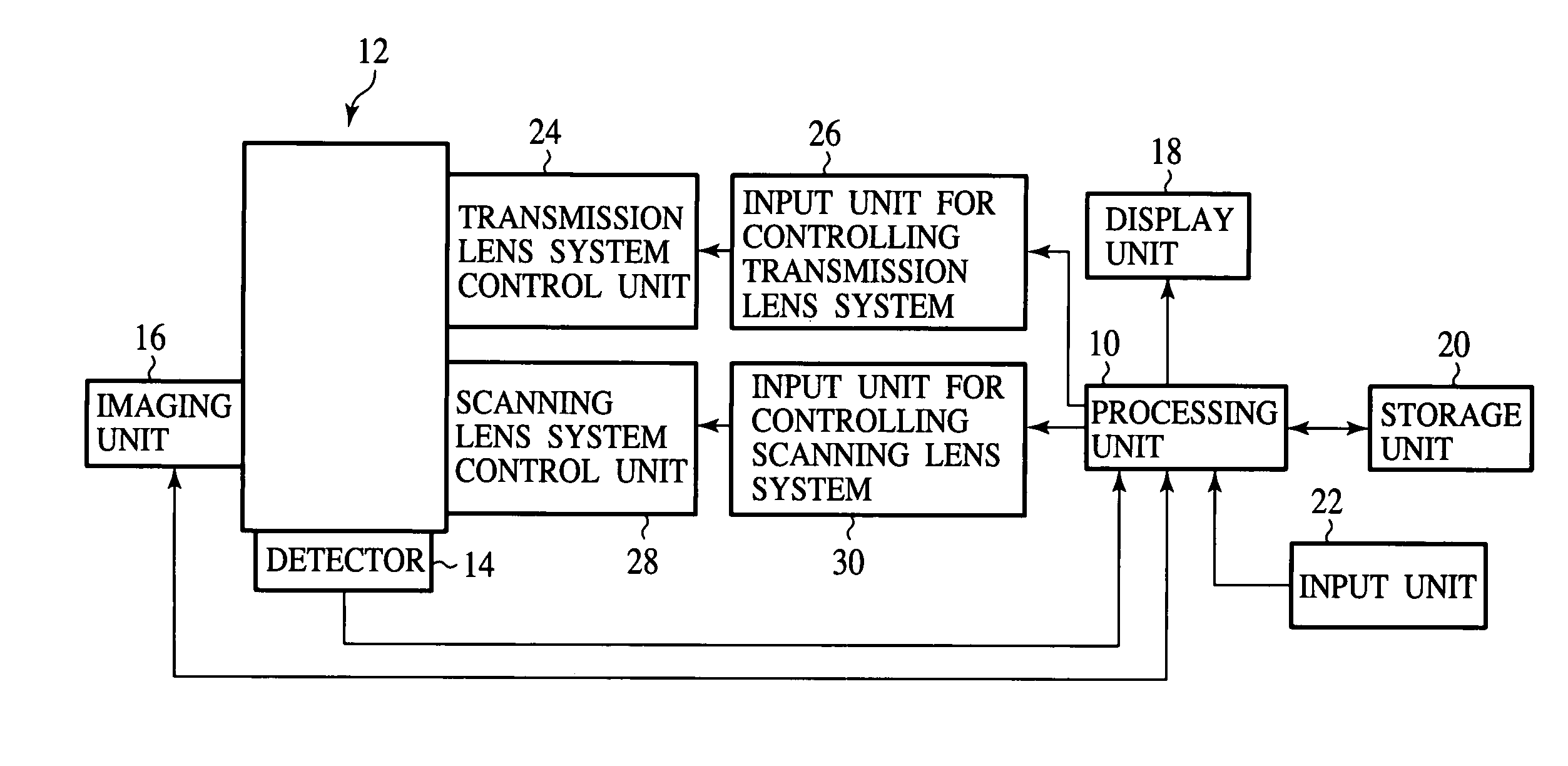
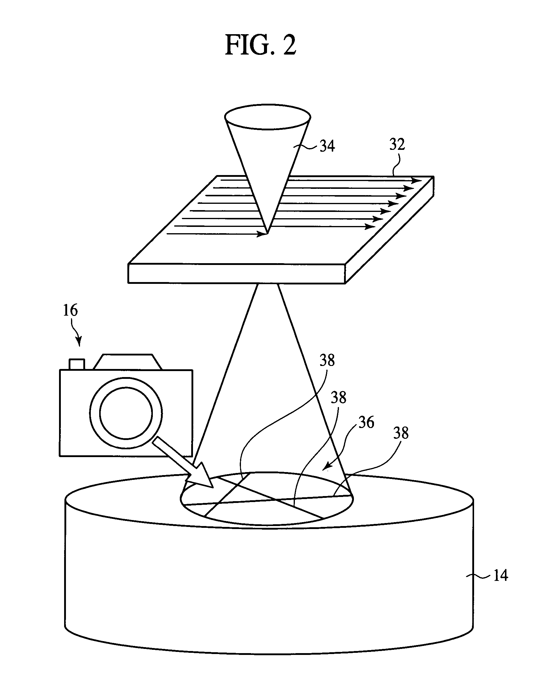
[0049]The lattice strain measuring system and method according to a first embodiment of the present invention will be explained with reference to FIGS. 1 to 6. FIG. 1 is a block diagram of the lattice strain measuring system according to the present embodiment. FIG. 2 is a view of a part of the lattice strain measuring system according to the present embodiment.

[0050](The Lattice Strain Measuring System)

[0051]The lattice strain measuring system according to the present embodiment will be explained with reference to FIGS. 1 and 2.

[0052]As shown in FIG. 1, the lattice strain measuring system according to the present embodiment comprises a processing unit 10 which generally controls the measuring system and performs prescribed processing, an STEM (Scanning Electron Transmission Microscope) 12, a detector 14 which is disposed below the part where a sample is to be mounted and detects magnitudes of electron beams transmitted by the sample, imaging unit 16 which takes pi...

second embodiment

A Second Embodiment

[0110]The lattice strain measuring system and method according to a second embodiment of the present invention will be explained with reference to FIGS. 1, 2, 7 and 8. The same member of the present embodiment as those of the lattice strain measuring system and method according to the first embodiment shown in FIGS. 1 to 6 are represented by the same reference numbers not to repeat or to simplify their explanation.

[0111]The lattice strain measuring system and method according to the present embodiment are characterized mainly in that relative lattice strain distributions are displayed.

[0112](The Lattice Strain Measuring System)

[0113]First, the lattice strain measuring system according to the present embodiment will be explained with reference to FIGS. 1 and 2.

[0114]In the present embodiment, a processing unit 10 computes respective finite differences between a lattice strain magnitude at a reference point and lattice strain magnitudes at respective measuring point...

third embodiment

A Third Embodiment

[0128]The stress measuring system and method according to a third embodiment of the present invention will be explained with reference to FIGS. 1, 2, 9 and 10. The same member of the present embodiment as those of the lattice strain measuring system and method according to the first or the second embodiment shown in FIG. 1 to 8 are represented by the same reference numbers not to repeat or to simplify their explanation.

[0129]The stress measuring system and method according to the present embodiment is characterized mainly in that stresses generated at respective measuring points are computed, based on lattice strain magnitudes given by the above-described method, and the image of a distribution of the computed stresses is displayed.

[0130](The Stress Measuring System)

[0131]First, the stress measuring system according to the present embodiment will be explained with reference to FIGS. 1 and 2.

[0132]A processing unit 10 computes stresses generated at respective measur...


PUM

PropertyMeasurementUnit
lattice strain distributionaaaaaaaaaa
lattice strainaaaaaaaaaa
scanning transmission electron microscopeaaaaaaaaaa

Abstract

A lattice strain measuring method including the steps of: using a scanning transmission electron microscope 12 to apply convergent electron beams 34 to a sample 32 and obtain a convergent-beam electron diffraction image 36 of the sample 32; computing a lattice strain magnitude of the sample 32, based on the obtained convergent-beam electron diffraction image; and displaying the computed lattice strain magnitude, associated with an electron microscope image of the sample 32. A scanning transmission electron microscope 12 is used, whereby electron beams 34 are caused to scan to thereby suitably set an incidence position. Accordingly, the incidence position of the electron beams can be displaced at a nanometer-order pitch accurately in a short period of time. The use of a scanning transmission electron microscope 12 requires no image forming lens below the sample 32, and the convergent-beam electron diffraction image is free from the distortion due to the influence of an image forming lens. Thus, a distribution of lattice strains in an electronic device having, e.g., a micronized structure can be displayed in an image with high resolving power and with high accuracy and furthermore in a short period of time.

Description

CROSS-REFERENCE TO RELATED APPLICATION[0001]This application is based upon and claims priority of Japanese Patent Application No. 2003-358403, filed on Oct. 17, 2003, the contents being incorporated herein by reference.BACKGROUND OF THE INVENTION[0002]The present invention relates to a lattice strain measuring system and method, and a stress measuring system and method.[0003]Lattice strains generated in a crystalline material affect various properties of the crystalline material. Lattice strains are an important factor which much influences device characteristics especially of highly integrated and micronized ultra LSIs.FIELD OF THE INVENTION[0004]Conventionally, lattice strains have been measured by X-ray diffraction or Raman spectroscopy.DESCRIPTION OF THE RELATED ART[0005]However, these methods, whose spatial resolving power is coarse, can not be used to evaluate micronized electronic devices.[0006]Recently, a technique of evaluating lattice strains by the convergent-beam electro...

Claims


Application Information

Patent Timeline
Patent Type & Authority Patents(United States)
IPC IPC(8): H01J37/252G01N23/20G01N23/04G01L1/00G01N23/207H01J37/00H01J37/28
CPCG01N23/046H01J37/252G01N2223/419H01J2237/2802H01J2237/24585
Inventor SOEDA, TAKESHI
Owner FUJITSU LTD
Why Eureka
Try Eureka