In-module current source

a current source and in-module technology, applied in the field of in-module current sources, can solve the problems of performance errors or damage to circuits, the practical limitation factor of hss circuit packaging development, and the ability to control parasitic circuit elements, so as to achieve the effect of minimizing the loop inductan

Inactive Publication Date: 2006-08-01
IBM CORP
View PDF9 Cites 13 Cited by
  • Summary
  • Abstract
  • Description
  • Claims
  • Application Information

AI Technical Summary

Benefits of technology

[0006]Additionally, because loop inductance can be formed within feedback loop between the voltage regulator and the power plane (e.g., by mutual inductance between the ground planes) and because of impedance across the power plane, the voltage regulator must be positioned as close to the chip and the power plane as possible. More specifically, the first and second ground planes can be positioned horizontally within the carrier between the top surface of the carrier and the power plane. A first regulator via extends through the top surface of the carrier to the first ground plane, electrically connecting the voltage regulator to the first ground plane and the second ground plane. A second regulator via extends through the top surface of the carrier to the power plane, electrically connecting the regulator to the power plane, the first ground plane and the second ground plane. Thus, the first ground plane, the first regulator via, the second ground plane and the second regulator via form an inductance loop within the feedback loop between the voltage regulator and the power plane. This inductance loop resists changes in current flow to the power plane. Additionally, the first ground plane, the second ground plane and the power plane comprise conductive planes that provide a low impedance path between the voltage regulator and the semiconductor chip. To minimize loop inductance between the planes as well as to minimize the impedance effect across the power plane, the voltage regulator must be placed as close as possible to both the chip and the power plane. Positioning the regulator in this manner, allows the regulator to effectively make real-time adjustments to the current passing to the semiconductor chip.
[0009]Additionally, due to an inductance loop that may be formed within the feedback loop between the voltage regulator and the power plane (e.g., by mutual inductances between the ground planes) and due to impedance across the power plane, the voltage-regulated current should be adjusted from a position as close as possible to both the power plane and chip. This minimizes the loop inductance between the planes and the impedance effect on the current flowing to the chip. Thus, a steady flow of the voltage-regulated current can be maintained across the power plane and can be instantaneously deliverable to the semiconductor chip.

Problems solved by technology

Fluctuations in power may cause performance errors or damage the circuits.
Thus, the requirement for lower source impedance and the ability to control parasitic circuit elements are the practical limiting factors for HSS circuit packaging development.

Method used


Image

  • In-module current source
  • In-module current source
  • In-module current source

Examples


Embodiment Construction

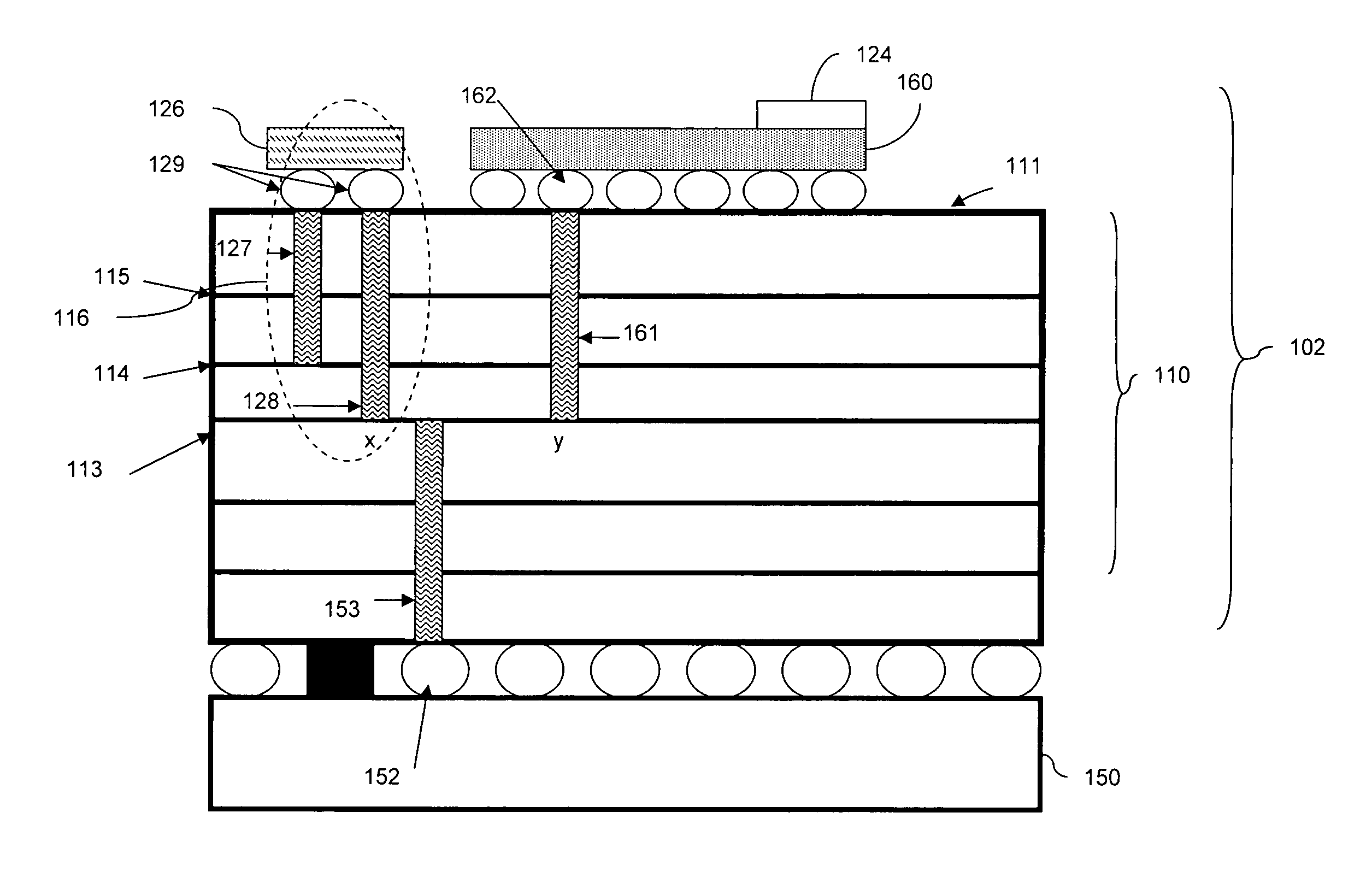
[0021]The present invention and the various features and advantageous details thereof are explained more fully with reference to the non-limiting embodiments that are illustrated in the accompanying drawings and detailed in the following description. It should be noted that the features illustrated in the drawings are not necessarily drawn to scale. Descriptions of well-known components and processing techniques are omitted so as to not unnecessarily obscure the present invention. The examples used herein are intended merely to facilitate an understanding of ways in which the invention may be practiced and to further enable those of skill in the art to practice the invention. Accordingly, the examples should not be construed as limiting the scope of the invention.

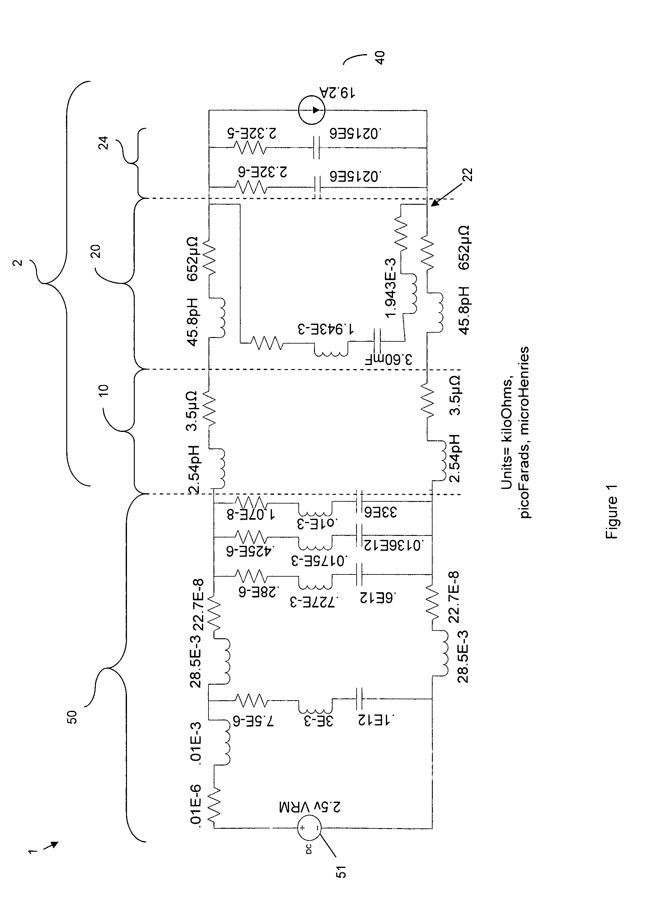
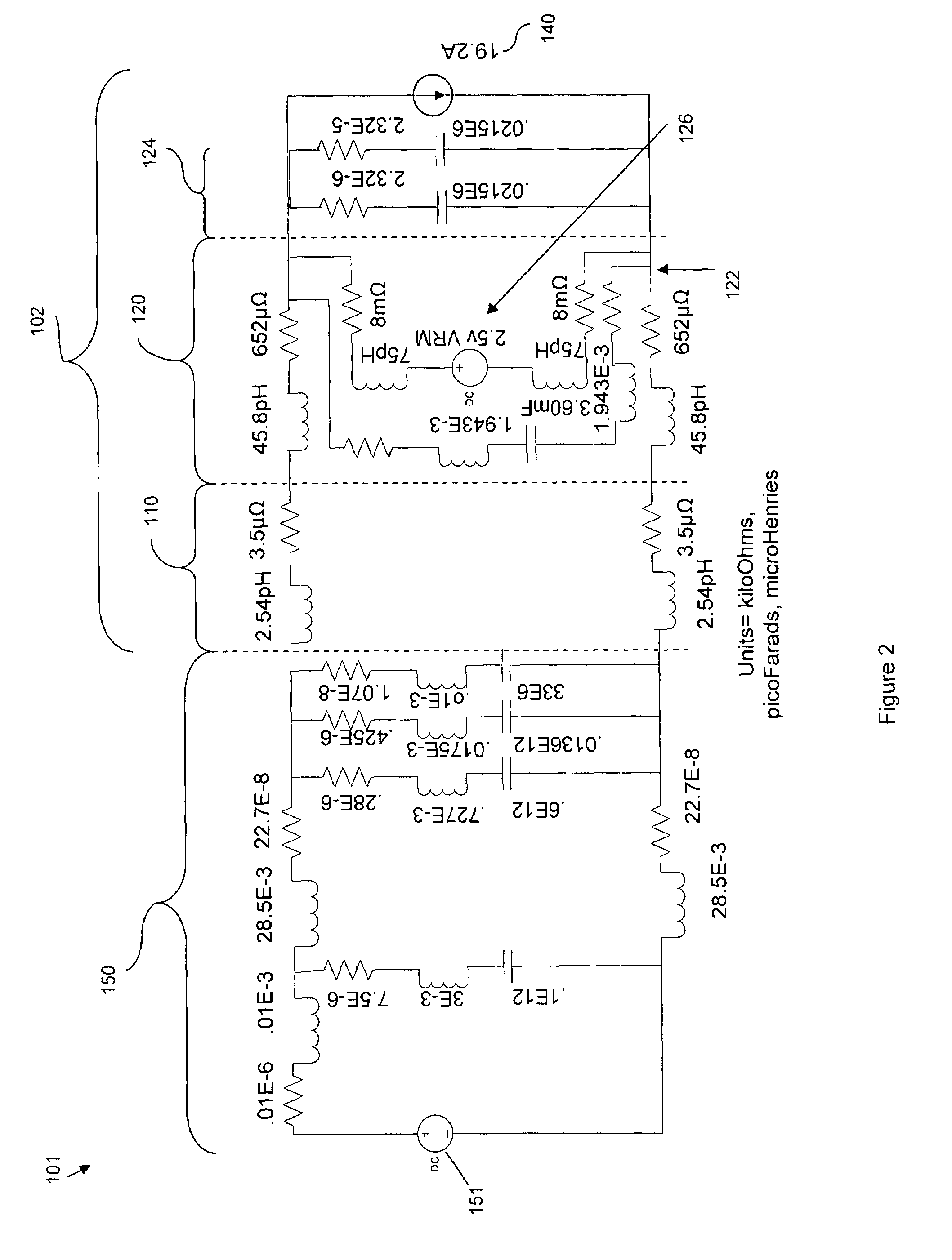
[0022]As stated above, the requirement for lower source impedance and the ability to control parasitic circuit elements are the practical limiting factors for HSS circuit packaging development. Providing sufficient power an...


PUM


Abstract

Disclosed is a method and structure for locally powering a semiconductor chip within a package. The structure and method incorporate a local voltage regulator mounted adjacent a semiconductor chip on a top surface of a carrier. The voltage regulator is electrically connected to a power plane disposed within the carrier. The voltage regulator continuously senses the reflected voltage of the power plane at a regulated output port and actively cancels time domain noise within its operational bandwidth. Mounting the voltage regulator on top of the carrier adjacent to the chip minimizes loop inductance between the regulator and power plane and also minimizes delay caused by impedance of the power plane on the current flowing to the chip.

Description

BACKGROUND OF THE INVENTION[0001]1. Field of the Invention[0002]The present invention relates to a semiconductor package and, more particularly, to a semiconductor package with a local voltage regulator to instantaneously provide a voltage-regulated current to power a chip within the semiconductor package.[0003]2. Description of the Related Art[0004]A semiconductor circuit module is an electrical component on which a chip, including a circuit or an integrated circuit is built. The circuit module can be mounted on a top surface of a specialized common carrier (SCC) that is encased within a semiconductor package for protection from the environment. The outer surface of the SCC can be electrically connected to a printed circuit board through conductive leads that extend through the bottom or sides of the SCC. The printed circuit board can connect the SCC to a power source, providing a current that can be distributed across the SCC to semiconductor chip interconnects. The integrated cir...

Claims


Application Information

Patent Timeline
Patent Type & Authority Patents(United States)
IPC IPC(8): H05K7/02H01L21/00H01L29/00
CPCH01L23/50H01L23/5383H01L23/5386H01L25/18H01L2224/16225H01L2924/15311H01L2924/3011H01L2924/00011H01L2924/00014H01L2224/0401
Inventor DYCKMAN, WARREN D.PILLAI, EDWARD R.O'CONNOR, DANIEL P.
Owner IBM CORP
Why Eureka
Try Eureka