Sample and hold circuit and bootstrapping circuits therefor

a hold circuit and sample technology, applied in the field of sample and hold circuits, can solve the problems of limiting the overall adc system performance of the s&h circuit, limiting the dynamic range of the circuit, and switching transients tending to degrade the performance of conventional s&h circuits, so as to improve the isolation of the hold mode, minimize the change, and improve the effect of settling tim

Active Publication Date: 2006-08-08
MICROELECTRONICS TECH INC
View PDF3 Cites 8 Cited by
  • Summary
  • Abstract
  • Description
  • Claims
  • Application Information

AI Technical Summary

Benefits of technology

[0008]The need in the art is addressed by the teachings of the present invention. In an illustrative embodiment, the teachings are embodied in a sample and hold circuit which is improved relative to the prior art. In an illustrative embodiment, the inventive sample, and hold circuit includes a first arrangement for receiving an input signal; a second arrangement for sampling and holding the signal in response to a control signal; and a third arrangement for minimizing a change in an input transistor's base current when the circuit switches from track to hold or hold to track. This offers improvements in settling time as current transients on an input terminal will not impact any driving circuit, such as a bandpass filter. In addition, it should increase the hold mode isolation thereby increasing the input dynamic range allowing distortion-free operation over a larger input negative voltage swing than per the designs of the prior art.
[0009]One feature is designed to hold the collector emitter (VCE) voltage constant at the input transistor. This should improve gain accuracy and linearity over the prior art where collector-emitter voltages are allowed to vary.
[0010]Another feature is designed to increase the dynamic current accuracy of a current mirror (M1 and M2) for a diode connected transistor QK, by holding M2's source to drain voltage, VSD, constant. This should keep the current in a current source constant so that it does not vary as a function of the input voltage thereby modulating the input signal. This should improve the accuracy and linearity of the sample and hold over the teachings of the prior art.
[0011]Yet another feature is designed to hold VCE constant for intermediate transistors (QF and QG below) resulting in improved gain accuracy and linearity. In one embodiment, a dummy leg is added to isolate the output voltage, VOUT, from switching transients that occur when an intermediate transistor (QH) is turned on at the transition from track to hold.

Problems solved by technology

If an ADC was perfect, then all errors associated with the conversion might be presumed to be caused by the S&H.
In reality, often the S&H performance is the limiting factor with respect to the overall ADC system performance.
First, switching transients tend to degrade the performance of conventional S&H circuits.
Second, the need to limit input voltage swings to avoid overdriving internal circuits tends to limit the dynamic range of the circuit.
Third, undesirable variations in gain, as a function of input voltage may cause, a nonlinearity over the input voltage range.
Fourth, variations in input voltage may cause other distortions and limit the dynamic range of the S&H.

Method used


Image

  • Sample and hold circuit and bootstrapping circuits therefor
  • Sample and hold circuit and bootstrapping circuits therefor
  • Sample and hold circuit and bootstrapping circuits therefor

Examples


Embodiment Construction

[0027]Illustrative embodiments and exemplary applications will now be described with reference to the accompanying drawings to disclose the advantageous teachings of the present invention.

[0028]While the present invention is described herein with reference to illustrative embodiments for particular applications, it should be understood that the invention is not limited thereto. Those having ordinary skill in the art and access to the teachings provided herein will recognize additional modifications, applications, and embodiments within the scope thereof and additional fields in which the present invention would be of significant utility.

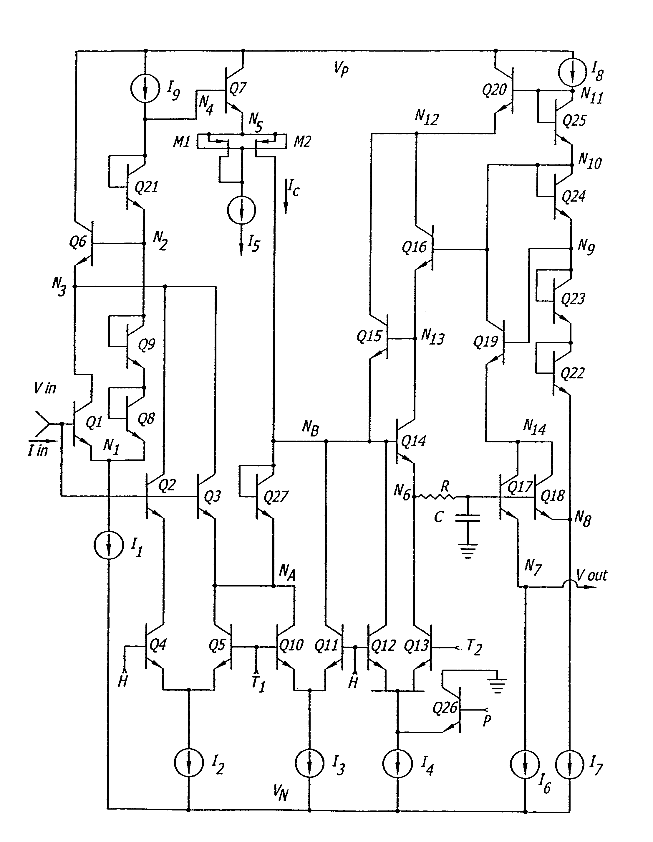
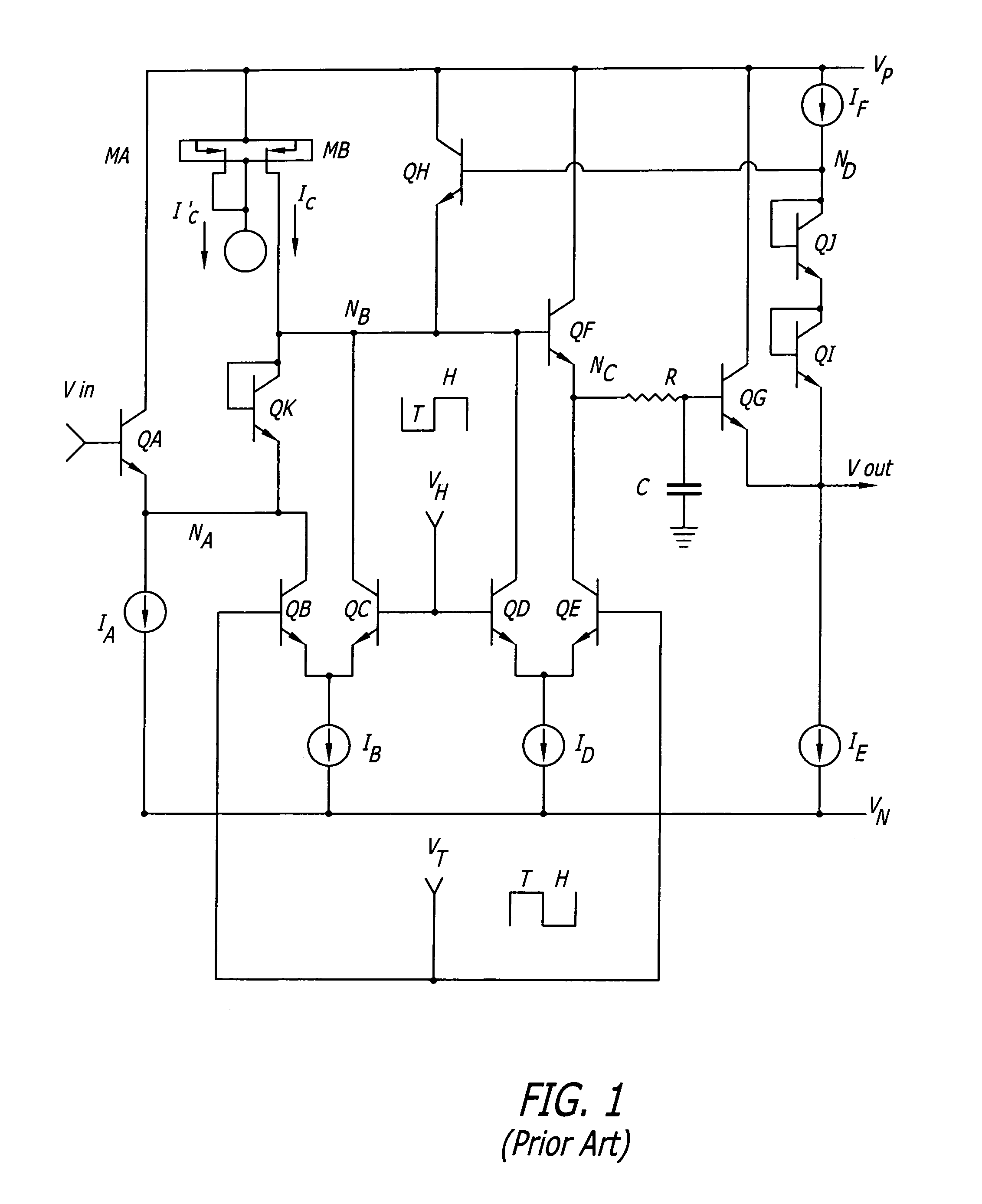
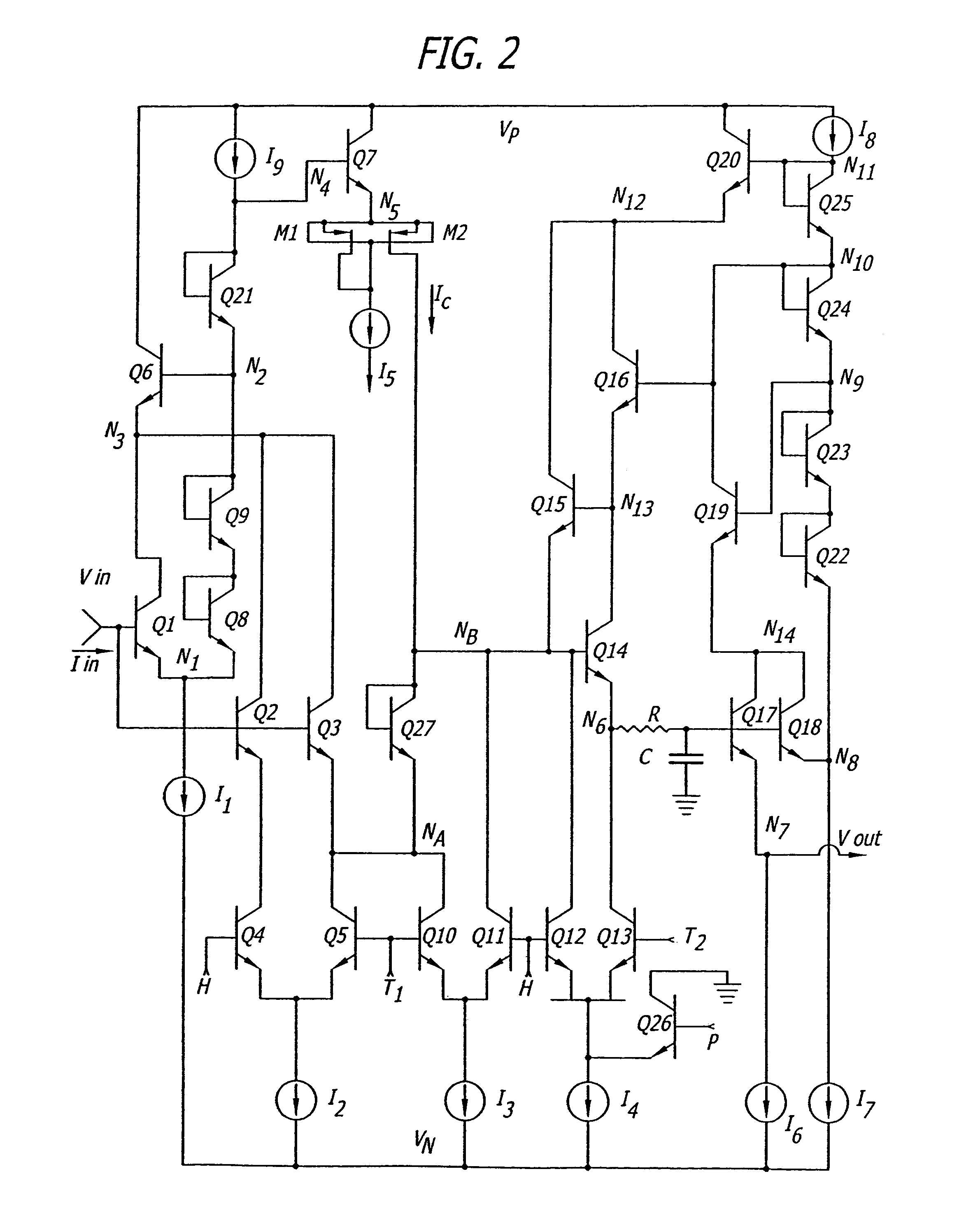
[0029]FIG. 1 is a typical implementation of a sample and hold (aka ‘track and hold’ circuit 10′ implemented in accordance with conventional teachings. In the present application, the terms ‘sample’ and ‘track’ are used interchangeably. In a track mode, VT is high and VH is low. Therefore QB and QE are conducting (on) and QC and QD are not conducting ...


PUM


Abstract

A sample and hold circuit including a first arrangement for receiving an input signal; a second arrangement for sampling and holding the signal in response to a control signal; and a third arrangement for minimizing the change in an input transistor's base current when the circuit switches from track to hold or hold to track and for keeping the collector emitter voltage constant at the input transistor. An arrangement is disclosed to increase the dynamic current accuracy of a current mirror for a diode connected transistor, by holding the voltage across one transistor in the current mirror constant. Another arrangement is disclosed for holding collector to emitter voltage constant for intermediate transistors resulting in improved gain accuracy and linearity. In one embodiment, a dummy leg is added to isolate the output voltage from switching transients that occur when an intermediate transistor is turned on at the transition from track to hold.

Description

CROSS-REFERENCE TO RELATED APPLICATIONS[0001]This application claims the benefit of U.S. Provisional Application No. 60 / 495,766, filed Aug. 14, 2003, the disclosure of which is hereby incorporated by reference.BACKGROUND OF THE INVENTION[0002]1. Field of the Invention[0003]The present invention relates to electrical and electronic circuits and systems. More specifically, the present invention relates to sample and hold circuits.[0004]2. Description of the Related Art[0005]Sample and hold (S&H) circuits are well-known in the art. S&H circuits store, on command, the instantaneous amplitude of an input signal. S&H circuits are used in a variety of applications including high-speed Analog to Digital Converters (ADCs). If an ADC was perfect, then all errors associated with the conversion might be presumed to be caused by the S&H. In reality, often the S&H performance is the limiting factor with respect to the overall ADC system performance. Therefore, it is important to optimize the S&H ...

Claims


Application Information

Patent Timeline
Patent Type & Authority Patents(United States)
IPC IPC(8): G11C27/02H03K5/00
CPCG11C27/02
Inventor DEVENDORF, DON C.LINDER, LLOYD F.TRAN, KELVIN T.
Owner MICROELECTRONICS TECH INC
Why Eureka
Try Eureka