End-of-range defect minimization in semiconductor device

a technology of semiconductor devices and defects, applied in the field of minimizing end-of-range defects and junction leakage, can solve the problems of junction leakage and end-of-range defects formation, and achieve the effect of significantly reducing junction leakage as a result of end-of-range defects

Active Publication Date: 2006-08-15
CONVERSANT INTPROP MANAGEMENT INC
View PDF4 Cites 13 Cited by
  • Summary
  • Abstract
  • Description
  • Claims
  • Application Information

AI Technical Summary

Benefits of technology

[0010]By partially re-crystallizing only shallower portions of the deep amorphous regions, a buffer is formed between the shallower, intermediate amorphous regions and the end-of-range defects located beyond the periphery of the original deep amorphous regions. The dopants are deeply implanted within the intermediate amorphous regions, and not beyond. High dose laser thermal annealing (LTA), for example, may be used to selectively melt to a depth not greater than that of the intermediate amorphous regions, to preserve the buffer region. The depth of the melt, therefore, will be at least as deep as the deep source / drain implants, but not greater than that of the intermediate amorphous regions. The source / drain junctions will be located at the depth of the melt. Consequently, the buffer is maintained between the junctions of the final source / drain regions and the end-of-range defects. Because the end-of-range defects are located away from the source / drain junctions, junction leakage as a result of the end-of-range defects is significantly reduced.

Problems solved by technology

A problem associated with source / drain regions is the formation of “end-of-range defects,” which are believed to stem from an interstitial-rich region proximate the lower portion of an amorphous silicon region.
When these end-of-range defects 60 are present in the source / drain regions 31, the defects disadvantageously cause junction leakage.

Method used


Image

  • End-of-range defect minimization in semiconductor device
  • End-of-range defect minimization in semiconductor device
  • End-of-range defect minimization in semiconductor device

Examples


Embodiment Construction

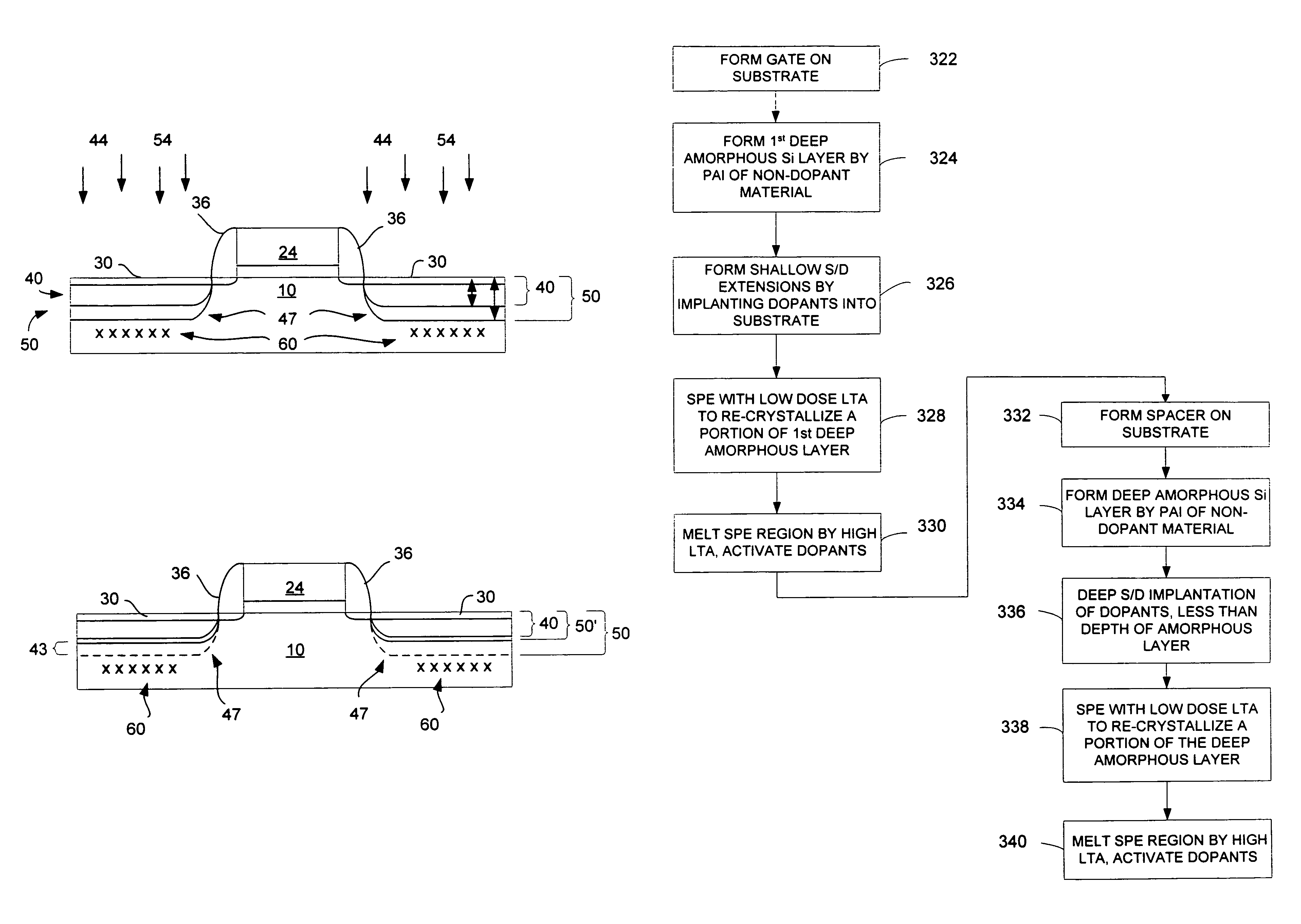
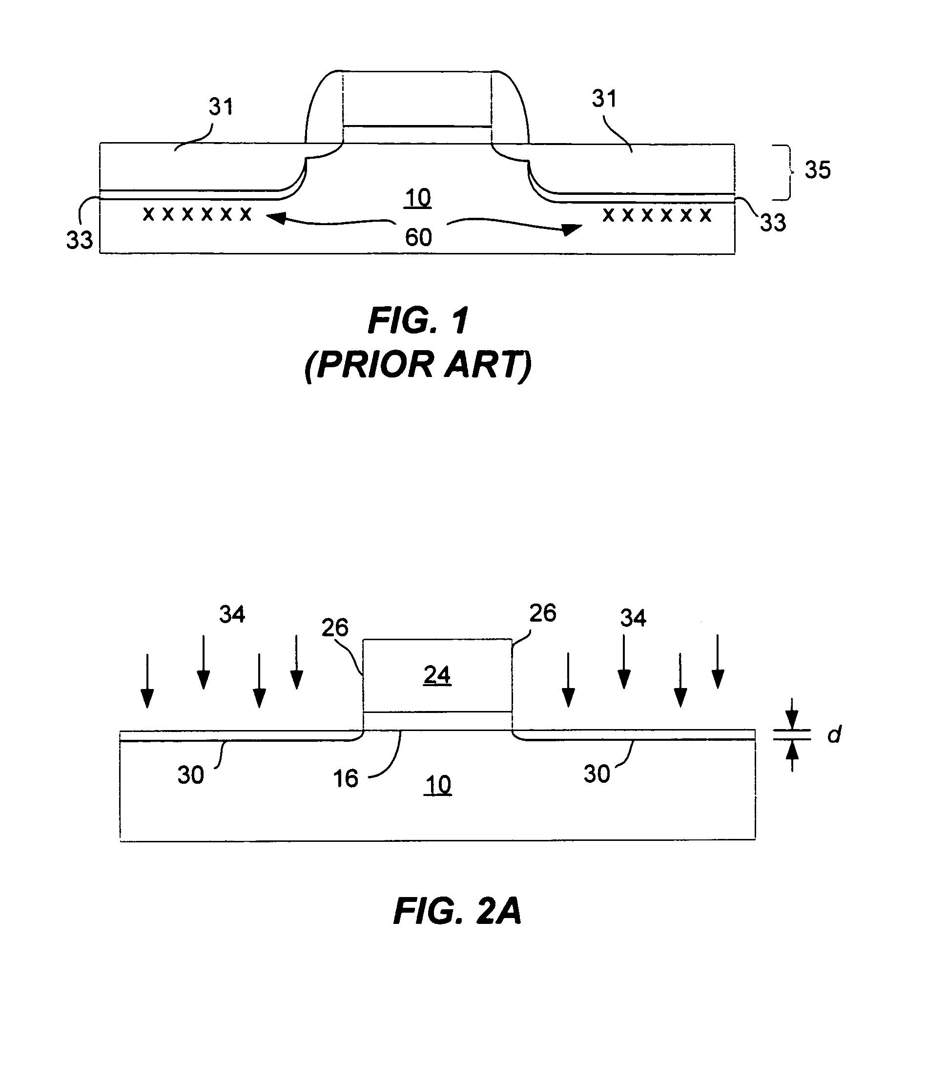
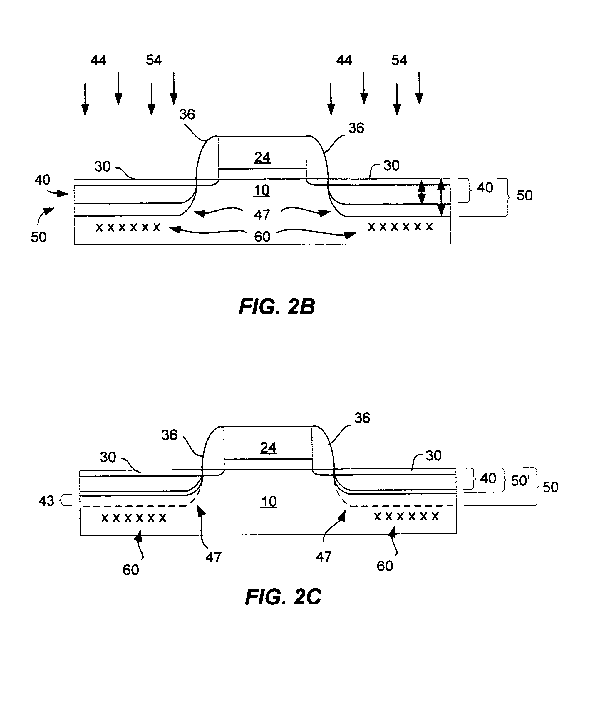
[0022]The present invention addresses and solves, at least in part, the problem of junction leakage as a result of end-of-range defects at the junctions of the source / drain regions of a semiconductor device. Various embodiments of the present invention may take the form of a method for fabricating a semiconductor device that leaves the end-of-range defects significantly deeper than the junctions of the active source / drain regions. The region between the end-of-range defects and active source / drain regions may be referred to as a “buffer”. The depths of various regions or layers provided herein are illustrative, and not meant to be restrictive. It is the relative depths of the regions and layers discussed herein that is significant.

[0023]In any of the various inventive methods, a gate electrode may be formed on a substrate, as is customary. Such methods also comprise forming deep amorphous silicon regions by pre-amorphitization implantation (PAI) within the substrate. Source / drain re...


PUM

PropertyMeasurementUnit
depthaaaaaaaaaa
depthaaaaaaaaaa
depthaaaaaaaaaa

Abstract

A method of fabricating a semiconductor device comprises forming a gate electrode over a substrate and forming deep amorphous regions within the substrate. And implanting dopants to form deep source/drain regions at a depth less than that of the deep amorphous regions, partially re-crystallizing portions of the deep amorphous regions to reduce their depth, and re-crystallizing the reduced amorphous regions to form activated final source/drain regions.

Description

FIELD OF THE INVENTION[0001]The present invention relates to the field of semiconductor device processing and manufacture, and more specifically, to minimizing end-of-range defects and junction leakage.BACKGROUND OF THE INVENTION[0002]A typical metal-oxide-semiconductor (MOS) device generally includes a semiconductor substrate on which a gate electrode is disposed. The gate electrode, which acts as a conductor, receives an input signal to control operation of the device. Source and drain regions are typically formed in regions of the substrate adjacent the gate electrodes by doping the regions with a dopant of a desired conductivity. The conductivity of the doped region depends on the type of impurity used to dope the region. The typical MOS transistor is symmetrical, in that the source and drain are interchangeable. Whether a region acts as a source or drain typically depends on the respective applied voltages and the type of device being made. The collective term source / drain regi...

Claims


Application Information

Patent Timeline
Patent Type & Authority Patents(United States)
IPC IPC(8): H01L21/336
CPCH01L21/26506H01L21/26513H01L29/7833H01L29/6659H01L21/268H01L21/2658
Inventor PATON, ERIC N.XIANG, QITABERY, CYRUS E.YU, BINOGLE, ROBERT B.
Owner CONVERSANT INTPROP MANAGEMENT INC
Why Eureka
Try Eureka