Semiconductor device and method of fabricating the same

a technology of semiconductor devices and semiconductor layers, applied in the direction of semiconductor devices, electrical equipment, transistors, etc., can solve the problems of junction leakage and resistivity increase of conventional semiconductor devices, and achieve the effect of reducing the junction leakage and lowering the resistivity of the silicide layer

Inactive Publication Date: 2009-11-26
RENESAS ELECTRONICS CORP
View PDF6 Cites 5 Cited by
  • Summary
  • Abstract
  • Description
  • Claims
  • Application Information

AI Technical Summary

Benefits of technology

[0022]The present invention can now provide a semiconductor device and a method of manufacturing the same, capable of suppressing spike of silicide layers formed over the source / drain impurity-diffused layers, or penetration of the contacts, and are thereby reduced in the junction leakage and lowered in the resistivity of the silicide layers.

Problems solved by technology

As described in the above, the conventional semiconductor devices have been suffering from increase in the junction leakage and resistivity, as a result of thinning of the silicide layers.

Method used


Image

  • Semiconductor device and method of fabricating the same
  • Semiconductor device and method of fabricating the same
  • Semiconductor device and method of fabricating the same

Examples


first embodiment

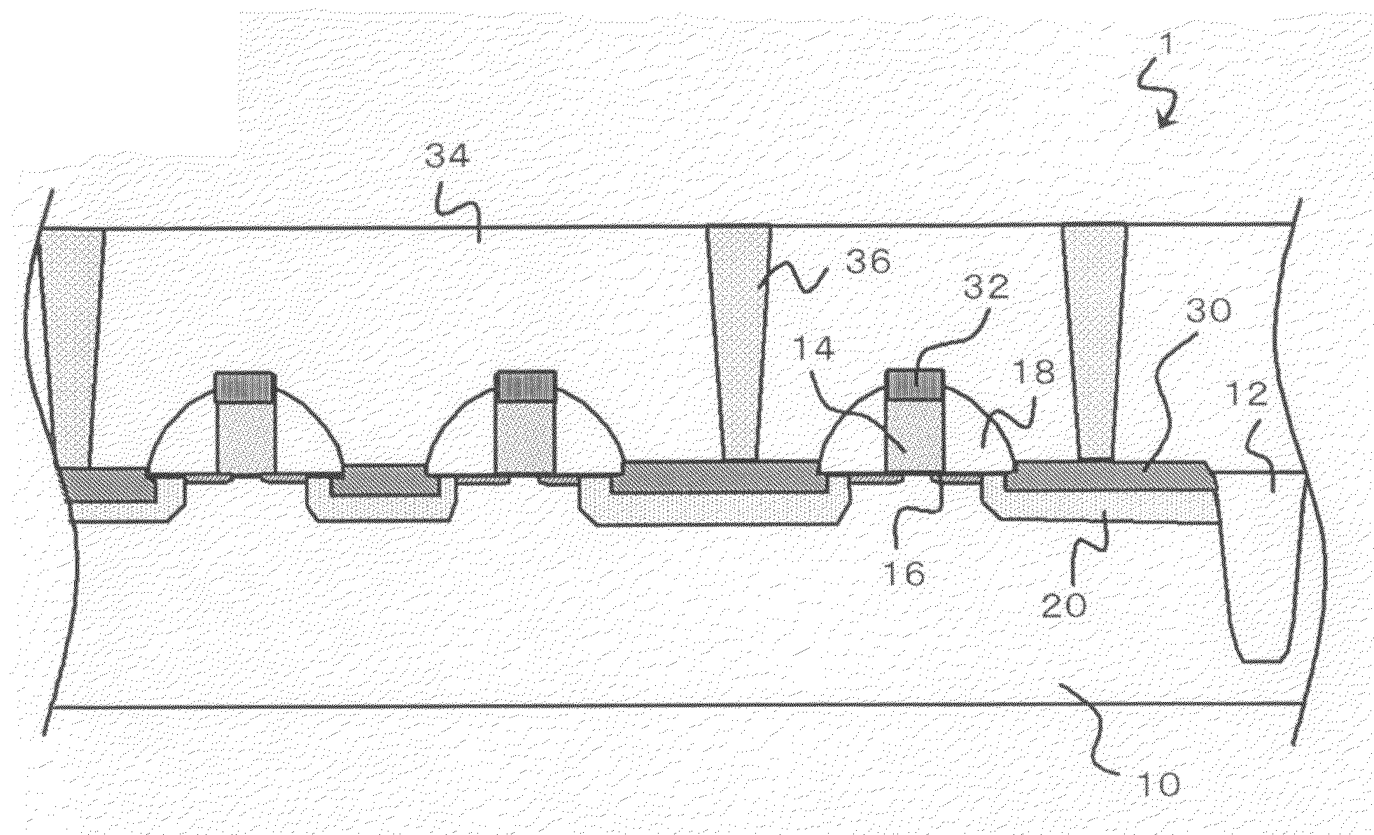
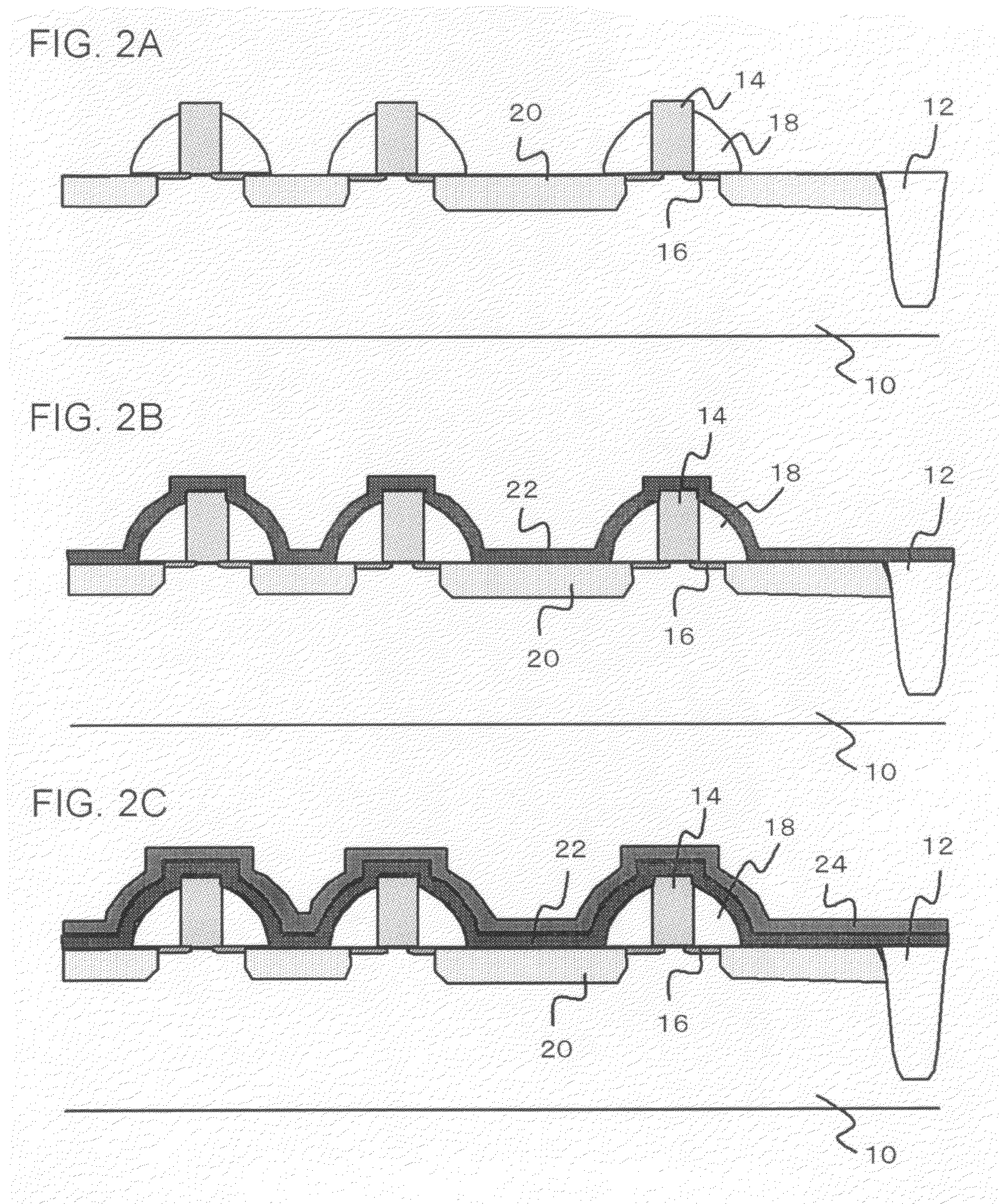
[0048]FIG. 1 is a sectional view illustrating a semiconductor device 1 of the first embodiment. The semiconductor device 1 has transistors formed on a semiconductor substrate 10. The gate electrode of each transistor is composed of a polysilicon electrode 14 and a silicide layer 32 formed thereon. The semiconductor device 1 further has low-concentration doped regions 16, source / drain impurity-diffused layers 20 composed of high-concentration doped regions, and silicide layers 30 formed over the source / drain impurity-diffused layers 20. The surface of each silicide layer 30 is positioned above the surface of the semiconductor substrate 10. The silicide layers 30 contain a silicidation-suppressive metal, and have a concentration profile according to which the concentration of the silicidation-suppressive metal increases from the surface of each silicide layer 30 in the depth-wise direction of the substrate, over a region of each silicide layer 30 ranging from the surface thereof to a ...

second embodiment

[0082]A method of manufacturing a semiconductor device according to a second embodiment is same as that in the first embodiment, up to the step of forming the primary silicide layers 26, 28, and the step of removing the unreacted portions of Ni and Pt (FIG. 2A).

[0083]This embodiment differs from the first embodiment, only in that, after the unreacted portions of Ni and Pt are removed, a secondary silicide layer is formed by sputtering as illustrated in FIG. 4A.

[0084]More specifically, the unreacted portions of Ni and Pt are removed, and a silicon film 40 is formed over the entire surface by sputtering at room temperature (FIG. 4A). In this process, the silicon film 40 is formed also over the sidewalls 18 and STI 12.

[0085]Next, the product is annealed at 500° C. for 30 seconds, so as to allow Ni and Pt to diffuse from the primary silicide layers 26, 28 to the silicon film 40, to thereby form the secondary silicide layers. The unreacted portions of the silicon film are then removed by...

third embodiment

[0093]A semiconductor device of a third embodiment is same as that in the second embodiment, in that the secondary silicide layer is formed by sputtering.

[0094]The third embodiment is, however, different from the second embodiment, in that the sidewalls are made to have nearly vertical shape as illustrated in FIGS. 5A to 5C, so as to avoid deposition of the silicon film over the surface of the sidewalls.

[0095]A method of manufacturing according to this embodiment will be explained referring to FIGS. 5A to 5C.

[0096]The source / drain impurity-diffused layers 20 are formed as the high-concentration doped regions, similarly to as described in the first embodiment. Note that the sidewalls 42 are formed to a nearly vertical shape. According to the recent tendency towards further dimensional shrinkage of semiconductor devices, the width d of the sidewalls 42 (see FIG. 5A) is 25 to 30 nm in the 45-nm generation, and 20 nm or narrower in the 32-nm generation.

[0097]More specifically, the sidew...


PUM


Abstract

Provided is a semiconductor device including a transistor that has a silicide layer formed over a semiconductor substrate. The gate electrode of each transistor is composed of a polysilicon electrode and the silicide layer formed thereon. Each transistor further has source/drain impurity-diffused layers composed of low-concentration doped regions and high-concentration doped regions, and silicide layers formed over the source/drain impurity-diffused layers. The surface of each silicide layer is positioned above the surface of the semiconductor substrate. The silicide layers contain a silicidation-suppressive metal, and have a concentration profile of the silicidation-suppressive metal over a region of the silicide layers ranging from the surface to a predetermined depth, such as increasing the concentration from the surface of each silicide layer in the depth-wise direction of the semiconductor substrate.

Description

[0001]This application is based on Japanese patent application No. 2008-135836 the content of which is incorporated hereinto by reference.BACKGROUND[0002]1. Technical Field[0003]The present invention relates to a semiconductor device and a method of manufacturing the same, and in particular to a semiconductor device having a silicide layer and a method of manufacturing the same.[0004]2. Related Art[0005]In semiconductor elements, such as MOS transistors, composing semiconductor integrated circuits silicide layers are formed over the source / drain impurity-diffused layers and over the gate electrodes, in order to lower the contact resistance. Titanium silicide, cobalt silicide, nickel silicide and so forth are adoptable to the silicide layers. In particular in recent years, Pt-doped nickel silicide has been used in view of improving the heat resistance.[0006]Japanese Laid-Open Patent Publication No. 2007-067225 may be exemplified as a publicly-known literature disclosing a method of m...

Claims


Application Information

Patent Timeline
Patent Type & Authority Applications(United States)
IPC IPC(8): H01L29/78H01L21/336
CPCH01L21/823418H01L29/7833H01L29/6659H01L29/665
Inventor IWAMOTO, TOSHIYUKI
Owner RENESAS ELECTRONICS CORP
Why Eureka
Try Eureka