Inductor for semiconductor integrated circuit and method of fabricating the same

a semiconductor integrated circuit and integrated circuit technology, applied in the field of inductors, can solve the problems of poor film planarization, difficult to improve the q value that indicates the performance of the inductor, and the inability of the conventional inductor to have a large cross-sectional area, so as to improve the q value, reduce resistance, and widen the cross-sectional area

Inactive Publication Date: 2006-08-15
RENESAS ELECTRONICS CORP
View PDF3 Cites 14 Cited by
  • Summary
  • Abstract
  • Description
  • Claims
  • Application Information

AI Technical Summary

Benefits of technology

[0014]Accordingly, it is an object of the invention to provide an inductor for a semiconductor integrated circuit, which provides a wider cross-sectional area, significantly reduces the resistance to improve the Q value and has a highly uniform film thickness, and a method of fabricating the inductor.

Problems solved by technology

Because of the restrictions on the interconnection width and the film thickness, the conventional inductor cannot have a large cross-sectional area.
The conventional inductor disadvantageously has a high resistance which makes it difficult to improve the Q value that indicates the performance of the inductor.
Further, the surface, 33, of the interconnection 22 undergone CMP is recessed by dishing as shown in FIG. 2D, resulting in poor film planarization.
Due to a variation in conditions for CMP, the uniformness of the film thickness of the inductor is poor, which is likely to cause a variation in the characteristics.

Method used


Image

  • Inductor for semiconductor integrated circuit and method of fabricating the same
  • Inductor for semiconductor integrated circuit and method of fabricating the same
  • Inductor for semiconductor integrated circuit and method of fabricating the same

Examples


Embodiment Construction

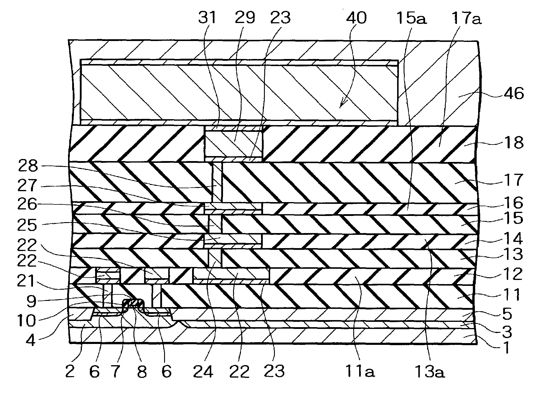
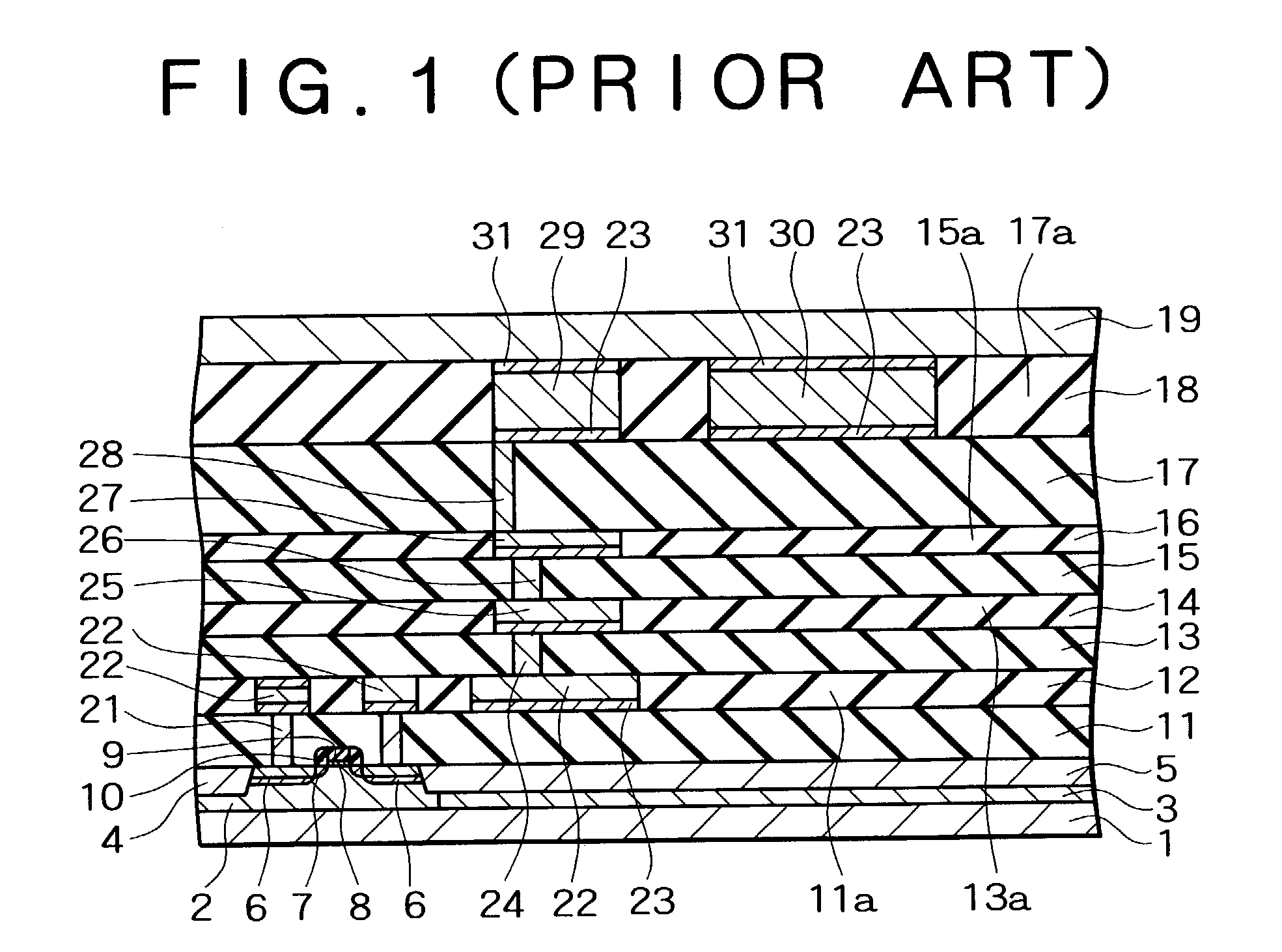
[0032]Preferred embodiments of the invention will be described below with reference to the accompanying drawings. FIG. 3 is a cross-sectional view illustrating an inductor according to the first embodiment of the invention, FIG. 4 is a perspective view showing the inductor portion in enlargement, and FIGS. 5A through 5D are cross-sectional views showing the fabrication process for the inductor step by step. To avoid the redundant description, like or same reference symbols are given to those structural elements in FIG. 3 which are the same as the corresponding elements shown in FIG. 1.

[0033]In FIG. 3, a multilayer interconnection is formed on a substrate 1 by the damascene method and the inductor in FIG. 3 is the same as the conventional inductor for a semiconductor integrated circuit shown in FIG. 1 up to a point where a contact hole 28 is formed in the fourth interlayer insulation film 17 which is the topmost layer as an interlayer insulation film. An insulation film 17a is formed...


PUM


Abstract

Disclosed are an inductor for a semiconductor integrated circuit, which provides a wider cross-sectional area, significantly reduces the resistance to improve the Q value and has a highly uniform film thickness, and a method of fabricating the inductor. A spiral inductor is formed on a topmost interconnection layer of a multilayer interconnection layer formed by a damascene method. This inductor is formed by patterning a barrier metal layer on an insulation film, on which a topmost interconnection is formed, in such a way that the barrier metal layer contacts the topmost interconnection, then forming a protective insulation film on an entire surface of the barrier metal layer, forming an opening in that portion of the protective insulation film which lies over the barrier metal layer, forming a thick Cu film with the barrier metal layer serving as a plating electrode, and performing wet etching of the Cu film. This process can allow the inductor to be so formed as to be thick and have a wide line width.

Description

BACKGROUND OF THE INVENTION[0001]1. Field of the Invention[0002]The present invention relates to an inductor which is formed in a semiconductor integrated circuit and a method of fabricating the inductor.[0003]2. Description of the Related Art[0004]A conventional inductor provided in a semiconductor integrated circuit is formed on the same layer as the interconnection of the topmost layer of a multilayer interconnection formed by a damascene process (see Japanese Patent Laid-Open No. 2001-267320). FIG. 1 is a cross-sectional view of a semiconductor integrated circuit including a conventional inductor. Wells 2 and 3 are formed in the surface of a substrate 1, and a pair of high-concentration diffusion layers 6 of an MOS transistor and a low-concentration diffusion layer 7 lying between the diffusion layers 6 are formed in an area which is defined by device isolation regions 4 and 5 on the surface of the well 2. A gate insulation film 8 is formed on the substrate between the diffusion...

Claims


Application Information

Patent Timeline
Patent Type & Authority Patents(United States)
IPC IPC(8): H01L29/00H01L21/3213H01L21/02H01L21/768H01L21/822H01L23/522H01L23/532H01L27/04H01L27/08
CPCH01L21/76838H01L23/5227H01L27/08H01L28/10H01L23/53228H01L2924/0002H01L2924/00
Inventor YAMAMOTO, RYOTAFURUMIYA, MASAYUKIOHKUBO, HIROAKINAKASHIBA, YASUTAKA
Owner RENESAS ELECTRONICS CORP
Why Eureka
Try Eureka