Method for controlling accuracy and repeatability of an etch process

a technology of etch process and repeatability, which is applied in the direction of fluid pressure measurement, semiconductor/solid-state device testing/measurement, instruments, etc., can solve the problems of significant delay and hours in receiving corrective feedback for improving the accuracy and repeatability of etch process subsequently performed, and achieve the control of accuracy and repeatability of etch process, reduce and/or remove sidewall polymers, improve the accuracy and repeatability of device fabrication

Inactive Publication Date: 2006-08-22
APPLIED MATERIALS INC
View PDF18 Cites 39 Cited by
  • Summary
  • Abstract
  • Description
  • Claims
  • Application Information

AI Technical Summary

Benefits of technology

[0008]The present invention is a method for controlling accuracy and repeatability of an etch process. Embodiments of the invention are practiced on a processing platform (e.g. a cluster tool) wherein robust pre-etch and post-etch data may be obtained in-situ. The method includes the steps of obtaining pre-etched critical dimension (CD) measurements of a feature on a substrate, etching the feature; treating the etched substrate to reduce and / or remove sidewall polymers deposited on the feature during etching, and obtaining post-etched CD measurements. The CD measurements may be utilized to adjust the etch process to improved the accuracy and repeatability of device fabrication.
[0009]In another embodiment of the invention, a method for etching comprises measuring dimensions of portions of a patterned mask, trimming the patterned mask using a process recipe based on these measurements, etching one or more layers on a substrate using the trimmed patterned mask as an etch mask, measuring dimensions of etched structures, and adjusting the trimming recipe or / and the etch recipe for subsequent substrates based on the post-etch measurements. The post-etch measurements are performed using an optical scatterometry measuring technique after sidewall residues have been reduced. As such, the post-etch measurements may be performed immediately after the substrate has been etched (e.g., prior to any wet post-etch clean procedure) to provide the real time feedback and process monitoring data to be used for etching subsequent substrates. In one application, the method is used to control accuracy and repeatability of etching a gate structure of a field effect transistor.

Problems solved by technology

The wet stripping processes are performed ex-situ and, as such, there is a significant delay (e.g., 1–2 hours) for receiving corrective feedback for improving the accuracy and repeatability of etch processes subsequently performed.

Method used


Image

  • Method for controlling accuracy and repeatability of an etch process
  • Method for controlling accuracy and repeatability of an etch process
  • Method for controlling accuracy and repeatability of an etch process

Examples


Embodiment Construction

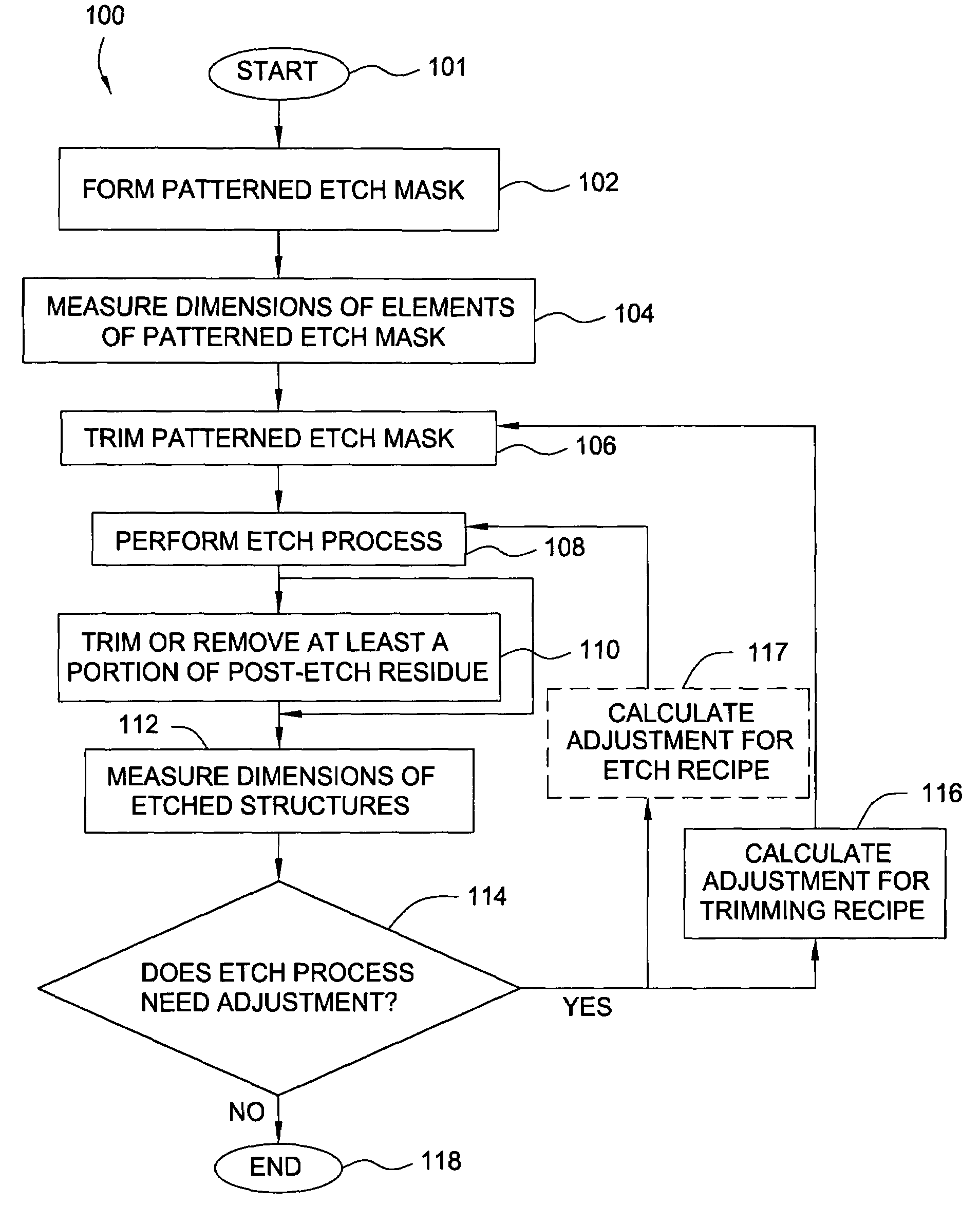
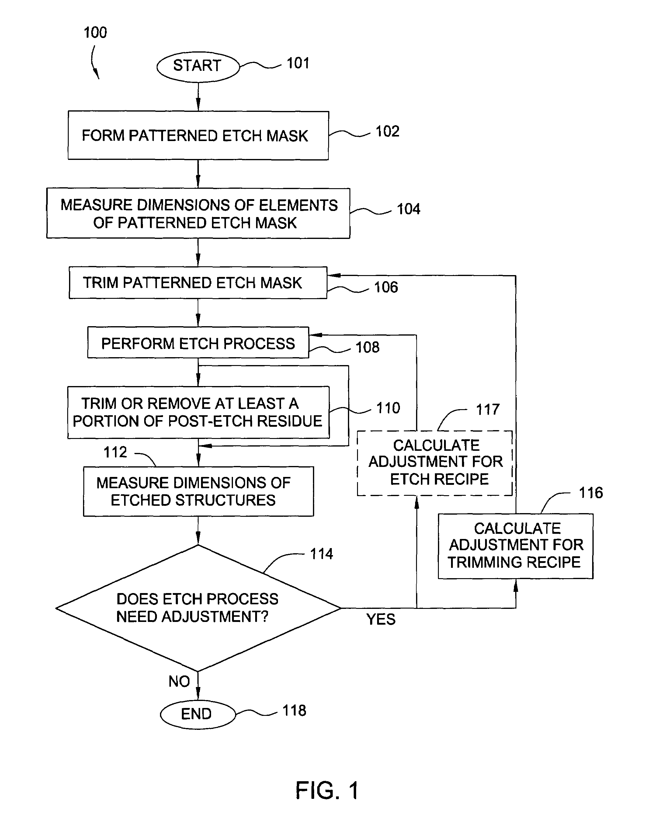
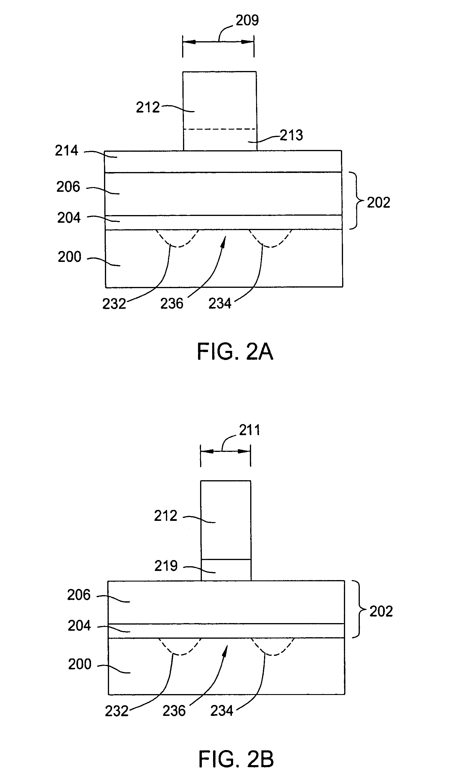
[0018]Embodiments of the invention generally relate to a method for etching in a processing platform (e.g., a cluster tool) wherein robust pre-etch and post-etch data may be obtained in-situ. The method includes the steps of obtaining pre-etched critical dimension (CD) measurements of a feature on a substrate, etching the feature, treating the etched substrate to reduce and / or remove sidewall polymers deposited on the feature during etching, and obtaining post-etched CD measurements. The CD measurements may be utilized to adjust the etch process to improved the accuracy and repeatability of device fabrication.

[0019]The present invention allows for the accuracy and precision of an etch process to be adjusted wafer to wafer, thereby enhancing process repeatability. The invention is generally used during fabrication of ultra-large-scale integrated (ULSI) semiconductor devices and circuits in a semiconductor substrate processing system.

[0020]FIG. 1 depicts a flow diagram of one embodime...


PUM

PropertyMeasurementUnit
thicknessaaaaaaaaaa
temperatureaaaaaaaaaa

Abstract

Embodiments of the invention generally relate to a method for etching in a processing platform (e.g. a cluster tool) wherein robust pre-etch and post-etch data may be obtained in-situ. The method includes the steps of obtaining pre-etched critical dimension (CD) measurements of a feature on a substrate, etching the feature; treating the etched substrate to reduce and / or remove sidewall polymers deposited on the feature during etching, and obtaining post-etched CD measurements. The CD measurements may be utilized to adjust the etch process to improved the accuracy and repeatability of device fabrication.

Description

BACKGROUND OF THE INVENTION[0001]1. Field of the Invention[0002]The present invention generally relates to semiconductor substrate processing systems. More specifically, the present invention relates to controlling accuracy and repeatability of etch processes in a semiconductor substrate processing system.[0003]2. Description of the Related Art[0004]To increase operational speed, devices (e.g., transistors, capacitors, and the like) in integrated microelectronic circuits have become ever smaller. One method for fabricating such devices comprises forming a patterned mask (e.g., photoresist mask) on a material layer disposed beneath such a mask (i.e., on an underlying layer) and then etching the material layer using the patterned photoresist mask as an etch mask. The etch mask generally is a replica of the structure to be formed (i.e., etched) in the underlying layer (or layers). As such, the etch mask has the same topographic dimensions as the structures being formed in the underlyin...

Claims


Application Information

Patent Timeline
Patent Type & Authority Patents(United States)
IPC IPC(8): H01L21/00H01L21/3065G03F7/20H01L21/02H01L21/302H01L21/311H01L21/3213H01L21/461
CPCH01L21/02071H01L21/32139H01L21/32137H01L21/31138
Inventor MUI, DAVIDLIU, WEISASANO, HIROKI
Owner APPLIED MATERIALS INC
Why Eureka
Try Eureka