Bidirectional shift register shifting pulse in both forward and backward directions

a technology of shift register and shift register, applied in the direction of digital storage, static storage, instruments, etc., can solve the problems of deteriorating display quality, variation, and inability to obtain the output signal of each shift register at a sufficient potential level

Active Publication Date: 2006-08-29
JAPAN DISPLAY CENTRAL CO LTD
View PDF5 Cites 66 Cited by
  • Summary
  • Abstract
  • Description
  • Claims
  • Application Information

AI Technical Summary

Benefits of technology

[0011]A bidirectional shift register of the first embodiment comprises an output circuit that includes a first transistor having a conductive path between a first clock terminal and an output terminal and a second transistor having a conductive path between a power supply electrode and the output terminal, an input circuit that includes a third transistor having a conductive path between a forward direction pulse input terminal and a control electrode of the first transistor, a fourth transistor having a conductive path between a backward direction pulse input terminal and the control electrode of the first transistor and a fifth transistor having a conductive path between the power supply electrode and a control electrode of the second transistor, a reset circuit that includes a sixth transistor having a conductive path between a second clock terminal and the control electrode of the second transistor, a seventh transistor having a conductive path between a third clock terminal and the control electrode of the second transistor and an eighth transistor having a conductive path between the power supply electrode and the control electrode of the first transistor, which makes the path between the sixth transistor, the control electrode of the second transistor and a control electrode of the eighth transistor conductive as well as making the path between the fifth transistor and the seventh transistor non-conductive in forward direction pulse shift and which makes the path between seventh transistor, the control electrode of the second transistor and the control electrode of the eighth transistor conductive as well as making the path between the fifth transistor and the sixth transistor non-conductive in backward direction pulse shift, and an inversion prevention circuit that prevents inversion of a voltage level in the control electrode of the second transistor when a voltage level of a clock signal inputted to the first clock terminal is inverted in a state where the first transistor is on and the second transistor is off.
[0012]According to this invention, in the forward direction pulse shift, the reset circuit makes the path between the sixth transistor, the control electrode of the second transistor and a control electrode of the eighth transistor conductive as well as making the path between the fifth transistor and the seventh transistor non-conductive. Thus through-current between the fifth transistor and the seventh transistor is prevented.
[0013]In the backward direction pulse shift, the reset circuit makes the path between seventh transistor, the control electrode of the second transistor and the control electrode of the eighth transistor conductive as well as making the path between the fifth transistor and the sixth transistor non-conductive. Thus through-current between the fifth transistor and the sixth transistor is prevented.
[0014]Moreover, by preventing the through-current, the potential of the control electrode of the second transistor is sufficiently increased and thus the eighth transistor and the second transistor reach a complete off state. The complete off state of the eighth transistor allows the first transistor to reach a complete on state. One of the first and second transistors is completely turned off and the both transistors are not simultaneously turned on. Thus, the potential level of the output signal can be stabilized, and it is possible to prevent variation in the potential level of the output signal between the forward direction pulse shift and the backward direction pulse shift.

Problems solved by technology

However, in the case of transmitting the pulse in a backward direction, an output signal of each shift register cannot be obtained at a sufficient potential level with the same circuit configuration as that in the case of the forward direction.
Thus, variation was a factor deteriorating display quality.

Method used


Image

  • Bidirectional shift register shifting pulse in both forward and backward directions
  • Bidirectional shift register shifting pulse in both forward and backward directions
  • Bidirectional shift register shifting pulse in both forward and backward directions

Examples


example

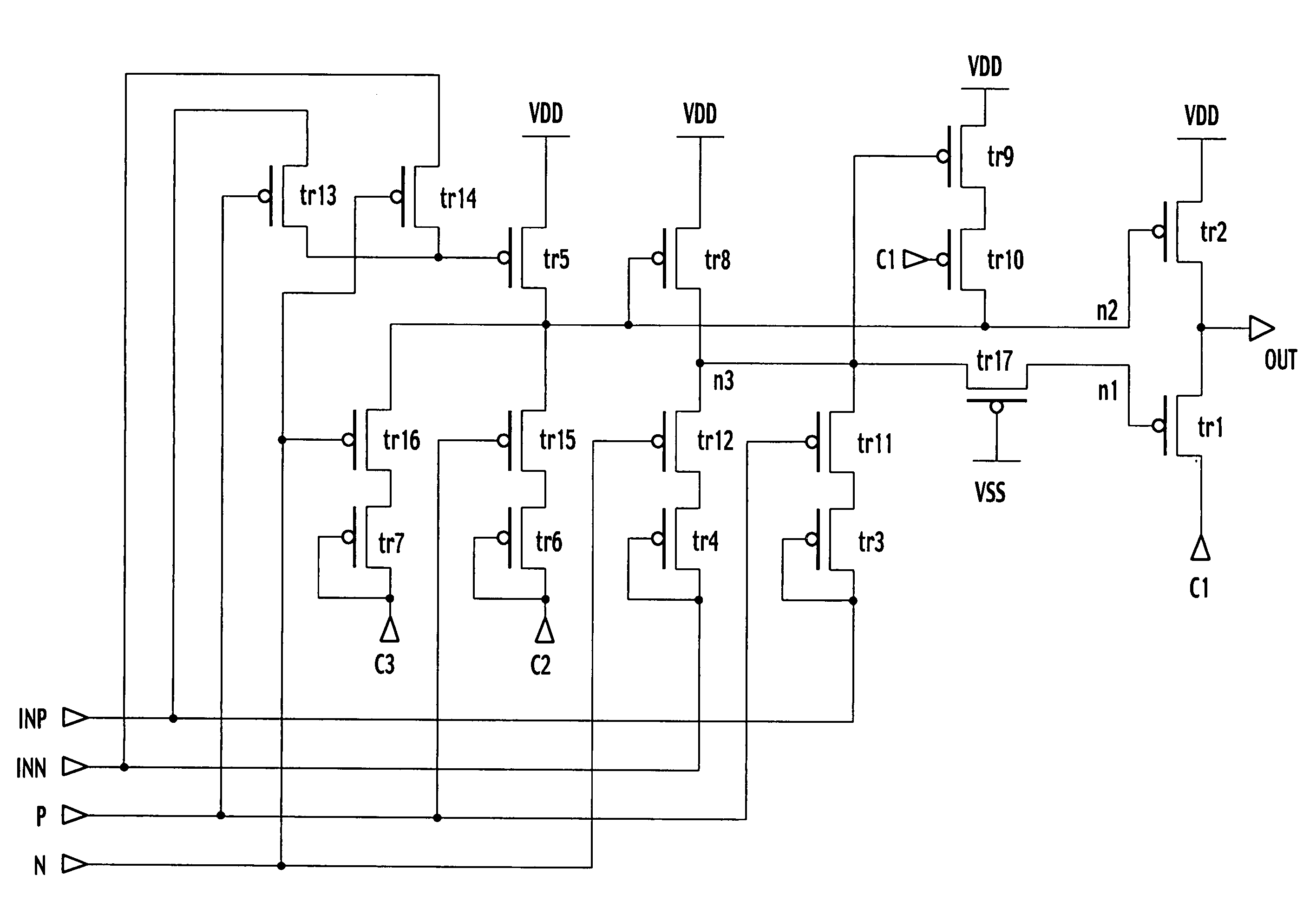
[0075]A bidirectional shift register DSR of an example is one that solves the above-described problems in the shift register of the comparative example. By use of the circuit diagram of FIG. 4 and timing charts of FIGS. 10 and 11, operations of the bidirectional shift register of the example will be described below. Here, it is assumed that the conductive path to the control electrode of the first transistor tr1 is the node n1, the conductive path to the control electrode of the second transistor tr2 is the node n2 and the conductive path to the source of the seventeenth transistor tr17 is the node n3.

[0076]Note that the first transistor tr1, the second transistor tr2, the third transistor tr3, the fifth transistor tr5, the sixth transistor tr6, the eighth transistor tr8, the ninth transistor tr9 and the tenth transistor tr10 of the bidirectional shift register DSR correspond to the twenty-first transistor tr21, the twenty-second transistor tr22, the twenty-third transistor tr23, th...


PUM

PropertyMeasurementUnit
conductiveaaaaaaaaaa
voltage levelaaaaaaaaaa
voltageaaaaaaaaaa

Abstract

In forward direction pulse shift, by turning off a sixteenth transistor, a through-current is prevented from flowing between the fifth transistor and the seventh transistor. In backward direction pulse shift, by turning off the fifteenth transistor, a through-current is prevented from flowing between the fifth and sixth transistors. Thus, a potential variation in an output signal of a shift register between the forward direction pulse shift and the backward direction pulse shift is prevented.

Description

CROSS-REFERENCE TO RELATED APPLICATIONS[0001]This application is based upon and claims the benefit of priority from Japanese Patent Application No. 2002-348831 filed on Nov. 29, 2002; the entire contents of which are incorporated herein by reference.BACKGROUND OF THE INVENTION[0002]1. Field of the Invention[0003]The present invention relates to a bidirectional shift register capable of shifting a pulse in both forward and backward directions and to a drive circuit and a flat display device, both of which use the bidirectional shift register.[0004]2. Description of the Related Art[0005]In recent years, a flat display device typified by a liquid crystal display device has been used in various kinds of equipment because the device is thin, lightweight and low in power consumption. In order to realize further thinning, weight saving and reduction in cost, a technology of configuring a drive circuit by use of polysilicon thin-film transistors with higher electron mobility than convention...

Claims


Application Information

Patent Timeline
Patent Type & Authority Patents(United States)
IPC IPC(8): G09G3/36G02F1/133G09G3/20G11C19/00
CPCG09G3/3677G09G3/3688G11C19/28G09G2310/0267G09G2310/0283G09G2310/0286G09G2320/02G09G2310/0275G09G3/36
Inventor KITANI, MASAKATSUMORITA, TETSUO
Owner JAPAN DISPLAY CENTRAL CO LTD
Why Eureka
Try Eureka