Semiconductor integrated circuit, design support apparatus, and test method

a technology of integrated circuits and support devices, applied in memory systems, program control, instruments, etc., can solve problems such as inability to obtain information necessary for analyzing failures, failures that are sometimes analyzed, and lengthen the design time required until scan becomes possibl

Inactive Publication Date: 2006-08-29
KK TOSHIBA
View PDF5 Cites 21 Cited by
  • Summary
  • Abstract
  • Description
  • Claims
  • Application Information

AI Technical Summary

Problems solved by technology

As a result, for an LSI having the failure, the failure is sometimes analyzed.
In this case, as described above, since the information indicating the presence / absence of the failure is compressed inside the LSI in the test using the logic BIST circuit, the information necessary for analyzing the failure cannot be obtained as such.
However, when the logic BIST circuit is used to analyze the failure as described above, there are several problems as follows.
Moreover, it is necessary to separately prepare the scan test pattern, and as a problem, a design time required until the scan becomes possible lengthens.
Therefore, the failure which can be detected only by a logic BIST operation cannot be analyzed.
This is an important problem, when an actual operation rate test is carried out by the logic BIST operation.

Method used


Image

  • Semiconductor integrated circuit, design support apparatus, and test method
  • Semiconductor integrated circuit, design support apparatus, and test method
  • Semiconductor integrated circuit, design support apparatus, and test method

Examples


first embodiment

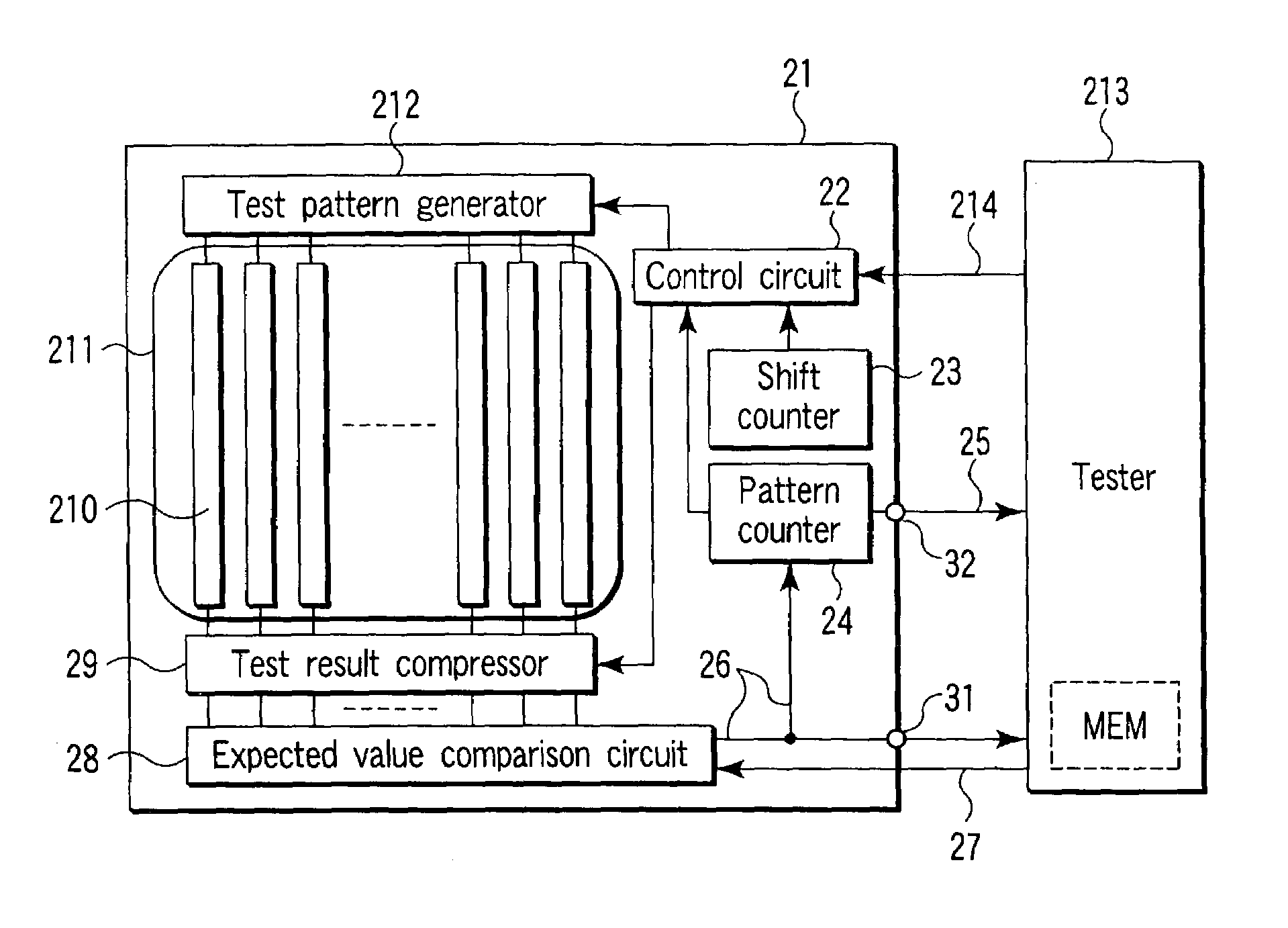
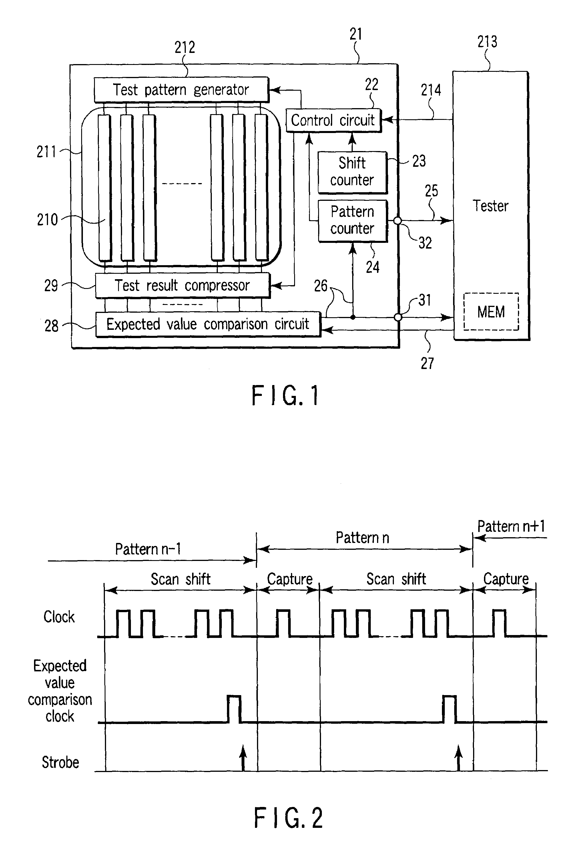
[0063]FIG. 1 is a block diagram showing a connection relationship between an LSI on which a logic BIST circuit is mounted according to a first embodiment of the present invention, and an external tester.

[0064]An LSI 21 is different from an LSI in which a usual logic BIST circuit shown in FIG. 16 is built in that a failure information output circuit is disposed to output from the LSI step information of a test pattern, when a failure is detected by logic BIST. Since the other respects are subsequently the same, the same parts of FIG. 1 as those of FIG. 16 are denoted with the same names.

[0065]In FIG. 1, the failure information output circuit is constituted, for example, of an expected value comparison circuit 28, first external terminal 31, and second external terminal 32. The expected value comparison circuit 28 compares a compressed value output from a test result compressor 29 with an expected value input from the tester outside the LSI for each test pattern, and outputs a failure...

second embodiment

[0084]FIG. 5 shows the connection relationship between the LSI on which the logic BIST circuit is mounted according to a second embodiment of the present invention, and the external tester.

[0085]This LSI 51 is different from the logic BIST circuit of the first embodiment shown in FIG. 1 in a test result compressor 511 which has a through function and failure information output circuit. The other constitution is subsequently similar to that of the first embodiment.

[0086]The test result compressor 511 having the through function includes a function of compressing data as the test result, and through function. In the through function, the signal supplied to the compressor 511 is directly output without being compressed.

[0087]Moreover, the failure information output circuit has a function of outputting step information of the test pattern and information of the register in a logic circuit 513 in which the failure is propagated to the outside of the LSI, when the failure is detected by t...

third embodiment

[0113]When the number (M) of internal scan chains of the block to be tested of the LSI is larger than the number (N) of pins of the tester, the number of internal scan chains needs to be adjusted to the number of pins of the tester in order to compare the expected values with each other every bit shift.

[0114]Alternatively, when the scan memory of the tester is used to supply the expected value to the logic BIST circuit, the number of scan paths inside the block to be tested is sometimes larger than the number of scan channels. In this case, the number of scan channels needs to be matched with the number of scan paths.

[0115]FIG. 9 shows the connection relationship between the LSI on which the logic BIST circuit of a selector type is mounted according to a third embodiment of the present invention, and the external tester.

[0116]This LSI 91 is different from the logic BIST circuit of the second embodiment shown in FIG. 5 in that the LSI 91 includes N selectors 917. These N selectors 91...


PUM


Abstract

A semiconductor integrated circuit includes a self-testing circuit having a test circuit which is incorporated in a logic circuit to test the logic circuit. The test circuit has a test pattern generator to generate a test pattern and a compressor to compress a test result output. The logic circuit includes a plurality of scan chains including a plurality of serial connected registers and the compressor includes a through output portion. The semiconductor integrated circuit also includes a pattern counter which counts the test pattern at a test time of the logic circuit, a shift counter which counts the number of shifts in the scan chain in the logic circuit at the test time, and a failure information output circuit which is connected to the test circuit and which outputs step information of the test pattern corresponding to a failure to an integrated circuit external terminal when the failure is detected at the test time.

Description

CROSS-REFERENCE TO RELATED APPLICATIONS[0001]This application is based upon and claims the benefit of priority from the prior Japanese Patent Application No. 2002-133186, filed May 8, 2002, the entire contents of which are incorporated herein by reference.BACKGROUND OF THE INVENTION[0002]1. Field of the Invention[0003]The present invention relates to a semiconductor integrated circuit (LSI), design support apparatus, and test method, particularly to a logic built-in self-test (BIST) circuit, design support apparatus, and test method, and is applied to, for example, a logic system LSI.[0004]2. Description of the Related Art[0005]As one of the test facilitating methods for solving the difficulty of testing a large and complicated LSI, a logic BIST is used. In the logic BIST, the generation of the test pattern given to a block to be tested, and analysis of the test result output from the block to be tested, are all automatically performed in the LSI by a logic circuit constituted in th...

Claims


Application Information

Patent Timeline
Patent Type & Authority Patents(United States)
IPC IPC(8): G06F9/44G01R31/3183G01R31/28G01R31/3185G06F17/50H01L21/822H01L27/04
CPCG01R31/318563G01R31/318569G01R31/318566
Inventor HASEGAWA, TETSUANZOU, KENICHI
Owner KK TOSHIBA
Why Eureka
Try Eureka