Method of manufacturing a longitudinal microsolenoid

Inactive Publication Date: 2006-09-19
NISHI TAKASHI
View PDF6 Cites 5 Cited by
  • Summary
  • Abstract
  • Description
  • Claims
  • Application Information

AI Technical Summary

Benefits of technology

[0013]According to the invention, an inductance value can easily be increased by controlling an occupied area of a coil in a substrate, and a change in a magnetic field can uniformly be maintained by retaining the magnetic flux within the coil.
[0014]Further, a solenoid coil can be formed on a microcircuit such as an integrated circuit or the like. And an integrated circuit having a small number of parts and having the stable characteristics of a circuit can be realized by connecting a single solenoid coil or plural coils having a required inductance performance. A high reliability with a small size can be expected from electronic appliances constructed of such an integrated circuit. And, the problem of delay that is expected from a larger-scale integrated circuit can be diminished by mounting solenoid coils in required positions.

Problems solved by technology

However, an inductance such as a solenoid coil involves many technical problems in that it is, in comparison with other elements, complex and difficult to manufacture.
Thus, the larger the number of transistors used, the more unstable the characteristics of the overall circuit tend to be.
Moreover, as the scale of the integrated circuit becomes larger, a wiring width of an electric wiring in the integrated circuit is more decreased, and the wiring route becomes longer, with the result that wiring resistance and the capacitance of wirings are increased.
Consequently, there arise problems such that the speed of charge passing through wiring is controlled, and the rate of delay of a current is increased.
Therefore, with this method, it is difficult to form a cylindrical section in the shape of a complete circle with high precision.
For this reason, a change in the magnetic field cannot be uniformly maintained.
Further, the technique disclosed in Japanese Patent Laid-Open No. 313,093 / 1998 is problematic, in that the spiral coil in which the upper and lower coils are spirally stacked via the through holes leaks a magnetic flux outside the coil in comparison with a solenoid coil, and a change in the magnetic field thus cannot be rendered uniform.

Method used


Image

  • Method of manufacturing a longitudinal microsolenoid
  • Method of manufacturing a longitudinal microsolenoid
  • Method of manufacturing a longitudinal microsolenoid

Examples


Embodiment Construction

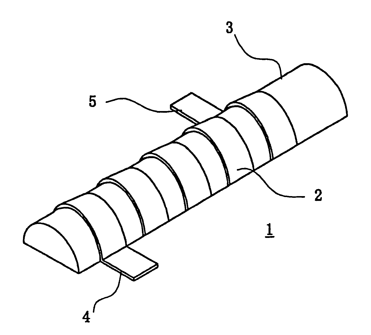
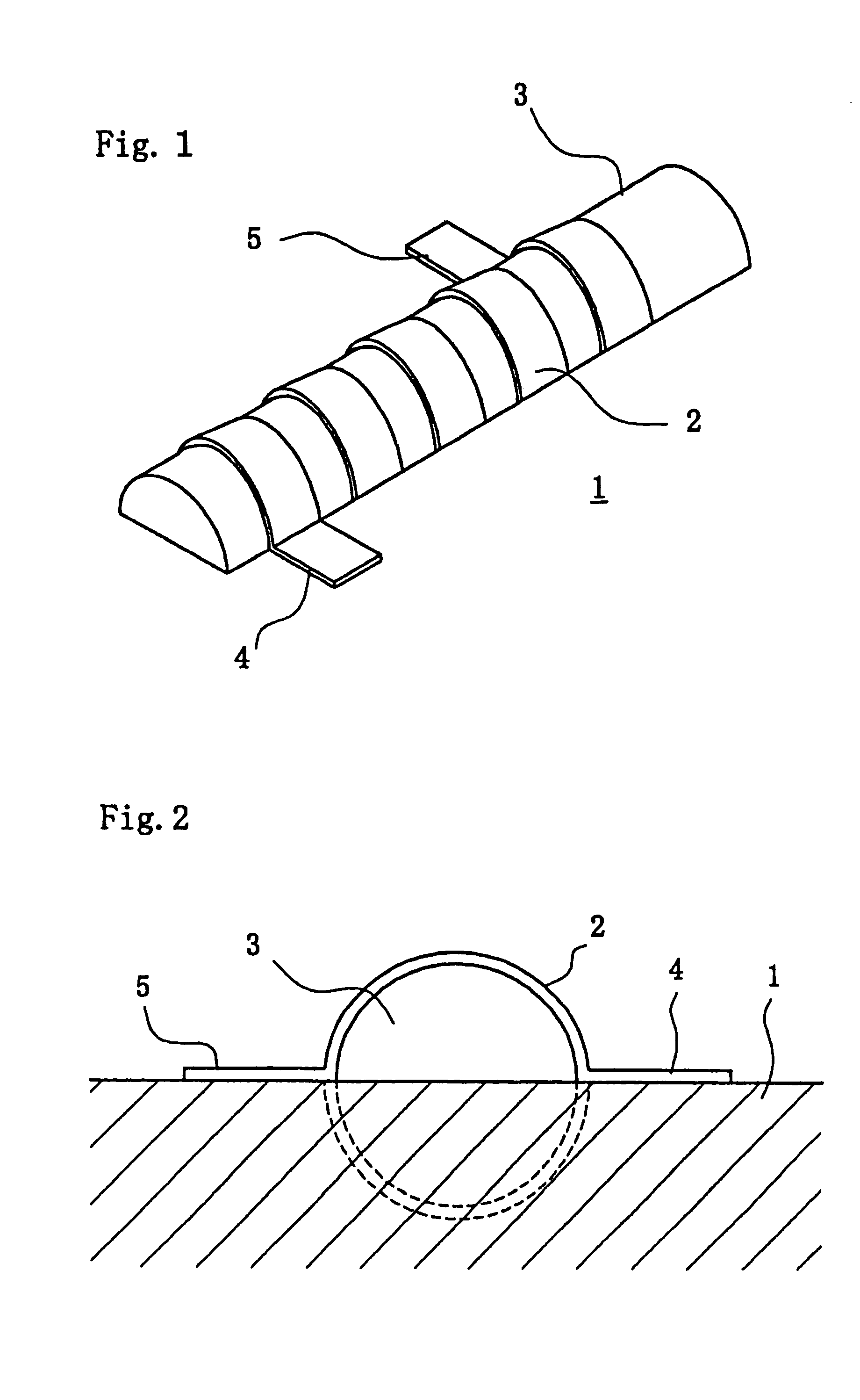
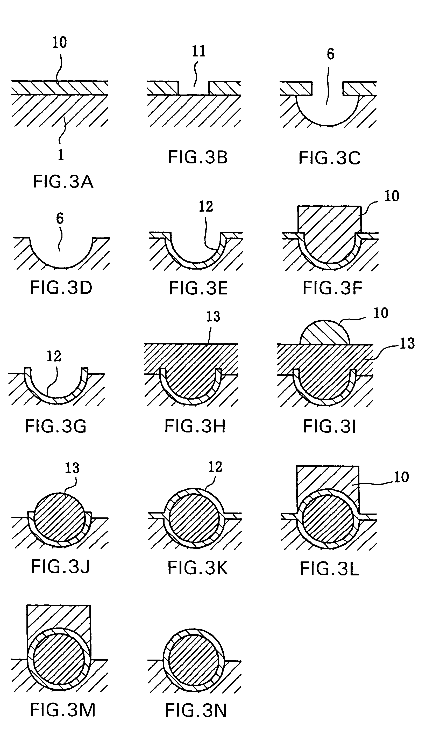
[0041]The invention is described more detail by referring to the drawings attached. Examples of the invention are explained by referring to the drawings. A method of manufacturing a microsolenoid coil using an ordinary semiconductor fine processing technique is explained by referring to the drawings. The microsolenoid coil of this Example is a lateral spiral coil (hereinafter simply referred to as a “spiral coil”) having a section of a complete circle. FIG. 1 is a perspective view of a lateral spiral coil manufactured by the method of the invention, and FIG. 2 is a side view of a lateral spiral coil manufactured by the method of the invention.

[0042]The lateral spiral coil has a structure such that a lower half coil portion 2 is formed on a groove bottom provided on a substrate 1 and has a section of a half of a complete circle, and such that an upper half coil portion 2 is formed on an outer peripheral surface of a cylindrical portion 3 protruded from the substrate 1, and such that ...


PUM

PropertyMeasurementUnit
Fractionaaaaaaaaaa
Fractionaaaaaaaaaa
Magnetic fieldaaaaaaaaaa

Abstract

A photosensitive material is coated on an insulating material (13) stacked on a substrate (1) (FIG. 16A), and exposed and developed using a mask having a light-shielding film capable of controlling a light transmittance from 100% to 0% annularly and continuously to form a spiral photosensitive material (FIG. 16B). After conducting treatment at a high temperature, the insulating material under the photosensitive material is spirally formed by etching (FIG. 16C). A metal (12) is stacked on the substrate (FIG. 16D), and a photosensitive material is coated (FIG. 16E). The photosensitive material is exposed and developed using a mask having an annular light-shielding film with a light transmittance of 0% to leave the photosensitive material covering only the metal on the base of the spiral structure (FIG. 16F). After treatment at a high temperature is conducted and the metal exposed is etched (FIG. 16G), the photosensitive material is removed (FIG. 16H).

Description

[0001]This is a division of application Ser. No. 09 / 914,542 filed Aug. 29, 2001, now U.S. Pat. No. 6,725,528.TECHNICAL FIELD[0002]The present invention relates to a microsolenoid coil which can be formed into a lateral or longitudinal spiral coil having a section of a circle that is nearly a complete circle by controlling exposure drawing on a photosensitive material, and a method of manufacturing the same.BACKGROUND OF THE INVENTION[0003]An inductance such as a solenoid coil or the like has often been used thus far in electric circuits other than microcircuits, such as in a semiconductor integrated circuit and the like. In microcircuits such as a semiconductor integrated circuit and the like, a transistor, a resistor, a condenser and the like are used. However, an inductance such as a solenoid coil involves many technical problems in that it is, in comparison with other elements, complex and difficult to manufacture.[0004]A schematic view of a projection exposure device used in a l...

Claims


Application Information

Patent Timeline
IPC IPC(8): H01F7/06H01F17/00H01F41/04
CPCH01F17/0033H01F41/041Y10T29/49156Y10T428/19Y10T428/149Y10T29/4902Y10T29/49073Y10T29/49155Y10T428/24
Inventor NISHI, TAKASHI
Owner NISHI TAKASHI
Why Eureka
Try Eureka