Electronic device

Inactive Publication Date: 2016-10-13
SILICONWARE PRECISION IND CO LTD
View PDF7 Cites 0 Cited by
  • Summary
  • Abstract
  • Description
  • Claims
  • Application Information

AI Technical Summary

Benefits of technology

The present invention uses a magnetically conductive element to increase the inductance of a single coil, which allows for the same inductance value as prior art using a reduced number of coils. This results in a smaller volume of the inductor.

Problems solved by technology

Such a limitation on the position of the passive elements reduces the routing flexibility.
Further, the position of the bonding pads limits the number of the passive elements mountable on the substrate, thereby hindering high integration of the semiconductor device.
As such, the semiconductor package is increased in volume and cannot meet the miniaturization requirement.
But such a method increases the bonding difficulty and complicates the fabrication process.
In addition, if the bonding wires 130 lack an effective support, the bonding wires 130 easily sag under gravity and come into contact with the inductor elements 12, thus causing a short circuit to occur.

Method used


Image

  • Electronic device
  • Electronic device
  • Electronic device

Examples


first embodiment

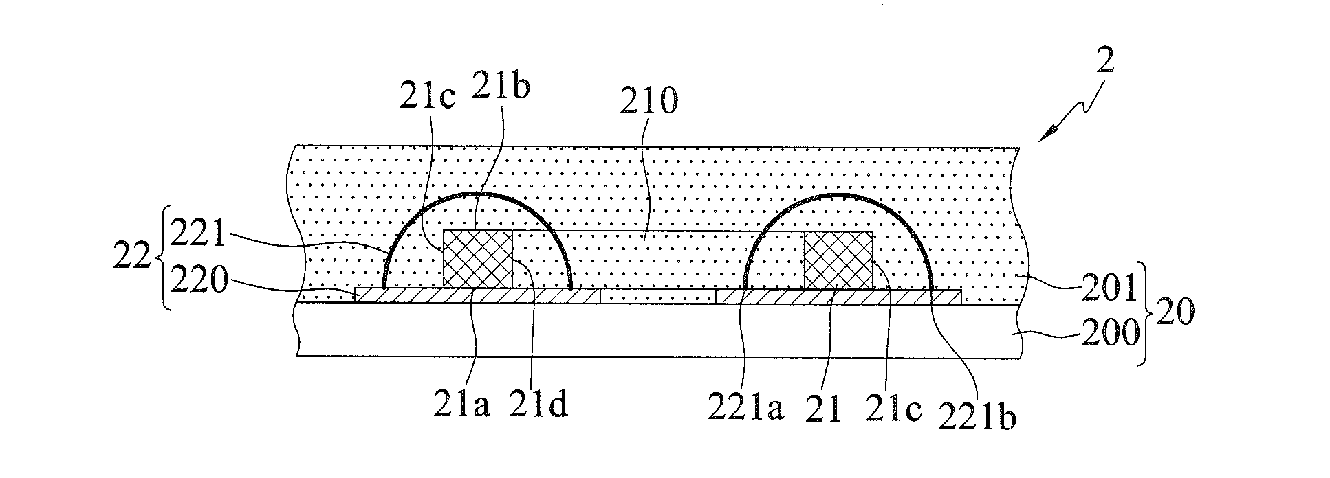
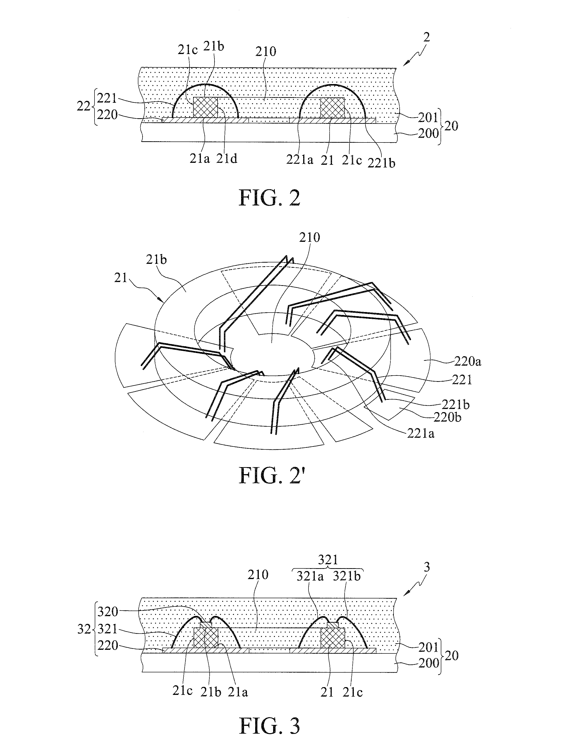
[0033]FIGS. 2 and 2′ show an electronic device 2 according to the present invention.

[0034]Referring to FIGS. 2 and 2′, the electronic device 2 has a magnetically conductive element 21, a conductor structure 22 formed around the magnetically conductive element 21, and a base body 20 encapsulating the magnetically conductive element 21 and the conductor structure 22.

[0035]The magnetically conductive element 21 has high permeability and is made of ferrite, Fe, Mn, Zn, Ni or an alloy thereof. The magnetically conductive element 21 has a first surface 21a, a second surface 21b opposite to the first surface 21a, an outer side surface 21c adjacent to and connecting the first surface 21a and the second surface 21b, and a through hole 210 communicating the first surface 21a and the second surface 21b. Therefore, the magnetically conductive element 21 has a ring shape. The wall surface of the through hole 210 constitutes an inner side surface 21d of the magnetically conductive element 21.

[003...


PUM


Abstract

An electronic device is provided, which includes: a magnetically conductive element having at least a through hole; a conductor structure formed on the magnetically conductive element and in the through hole; and a base body encapsulating the magnetically conductive element and the conductor structure, thereby allowing the electronic device to generate a higher magnetic flux and thus cause an increase in inductance.

Description

BACKGROUND OF THE INVENTION[0001]1. Field of the Invention[0002]The present invention relates to electronic devices, and more particularly, to an electronic device having a magnetically conductive element.[0003]2. Description of Related Art[0004]Along with the rapid development of electronic industries, electronic products are developed toward the trend of multi-function and high performance. To meet the miniaturization requirement of semiconductor packages, packaging substrates for carrying chips are becoming thinner. Further, the chips are required to have high-integration electronic circuits and high-density I / O connections to increase memory capacities and operating frequencies and reduce voltage requirements, thereby allowing the electronic products to become lighter, thinner, shorter, smaller and faster.[0005]In semiconductor application devices such as communication or high-frequency semiconductor devices, most RF passive elements such as resistors, inductors, capacitors and ...

Claims


Application Information

Patent Timeline
IPC IPC(8): H01F27/28H01F27/02
CPCH01F27/2804H01F2027/2809H01F27/022H01F17/062H01F2027/2814H01L2224/48091H01L2224/73265H01L2924/15311H01L2924/19105H01L2924/19107H01L2224/45144H01L2924/00014H01L2924/00
Inventor CHIU, CHIH-HSIENTSAI, CHI-PINTSAI, MING-FANJHANG, JYUN-YUANSHIH, CHI-LIANG
Owner SILICONWARE PRECISION IND CO LTD
Why Eureka
Try Eureka