Systems and methods for using non-contact voltage sensors and corona discharge guns

a voltage sensor and non-contact technology, applied in the field of microelectronic device manufacturing, can solve the problems of reduced production efficiency and device quality, low deposition rate, measured voltage including, etc., and achieve the effect of avoiding the use of ultra-high vacuum, accurate voltage measurements of substrates, and accurate values pertaining to electrical properties of substrates

Inactive Publication Date: 2006-09-19
KLA TENCOR TECH CORP
View PDF17 Cites 12 Cited by
  • Summary
  • Abstract
  • Description
  • Claims
  • Application Information

AI Technical Summary

Benefits of technology

[0020]There may be several advantages to using the systems and methods provided herein. For example, more accurate voltage measurements of substrates may be obtained due to the method and system presented fior calibrating the work function of a non-contact voltage sensor. As a result, more accurate values pertaining to electrical properties of the substrate may be obtained. Moreover, the methods and systems provided herein offer a manner with which to measure a voltage of a substrate using a non-contact voltage sensor in an ambient environment. Consequently, the use of ultra-high vacuums may be avoided. In addition, corona ions may be deposited in a more uniform and efficient manner with the corona gun configurations described herein. Furthermore, the length of a corona gun may be customized for individual operations, using the provided adaptations to alter the length of the corona gun.

Problems solved by technology

Inaccurate analysis of one or more parameters within a microelectronic device, such as a transistor, may hinder or prohibit the function of the device, leading to a reduction in production efficiency and device quality.
Conventional techniques that are able to deposit uniform charges, however, usually suffer from a low deposition rate.
As such, there is typically a trade-off between uniformity and deposition rate when using non-contact electrical testing techniques.
Another difficulty with non-contacting testing systems is that the measured voltage includes contributions not just from the surface to be measured, but also from the work function of the surface being measured and the work function of the sensor used for the measurement.
In ambient conditions, φms is difficult to determine and is a function of not only the material properties of the sensor and measured surface, but of ambient conditions such as temperature, humidity, water layers on the measured surface, partial pressures of various trace gases in the air, and air-borne molecular contamination. φms is also known to drift over extended periods of time.
For example, practical measurements of the stability of φms show that it is difficult to prevent drifts on the order of greater than about 10 mV over timescales of hours or several hundred mV over a longer time period.
Therefore, uncertainty in φms adds uncertainty to the measured voltage.
The exposure of the substrates to be measured, on the other hand, is limited and is usually consistent since they are measured at the same point in the fabrication process.
Unfortunately, however, an ultra-high vacuum environment is typically costly and difficult to maintain, making the use of such an environment impractical for many applications.

Method used


Image

  • Systems and methods for using non-contact voltage sensors and corona discharge guns
  • Systems and methods for using non-contact voltage sensors and corona discharge guns
  • Systems and methods for using non-contact voltage sensors and corona discharge guns

Examples


Embodiment Construction

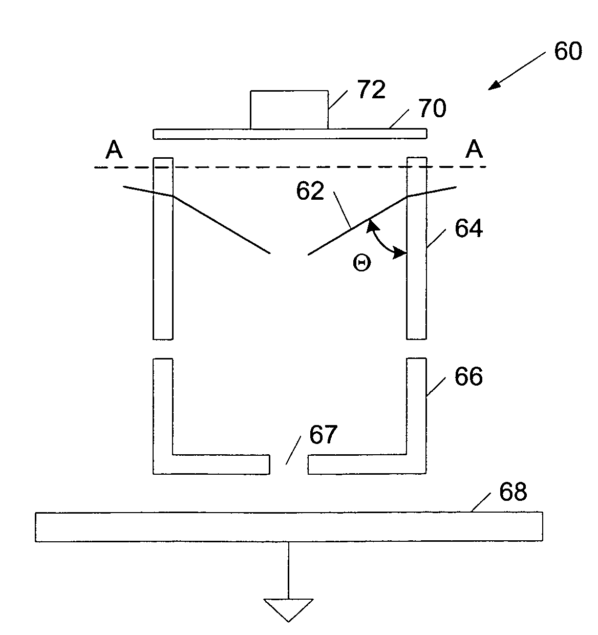
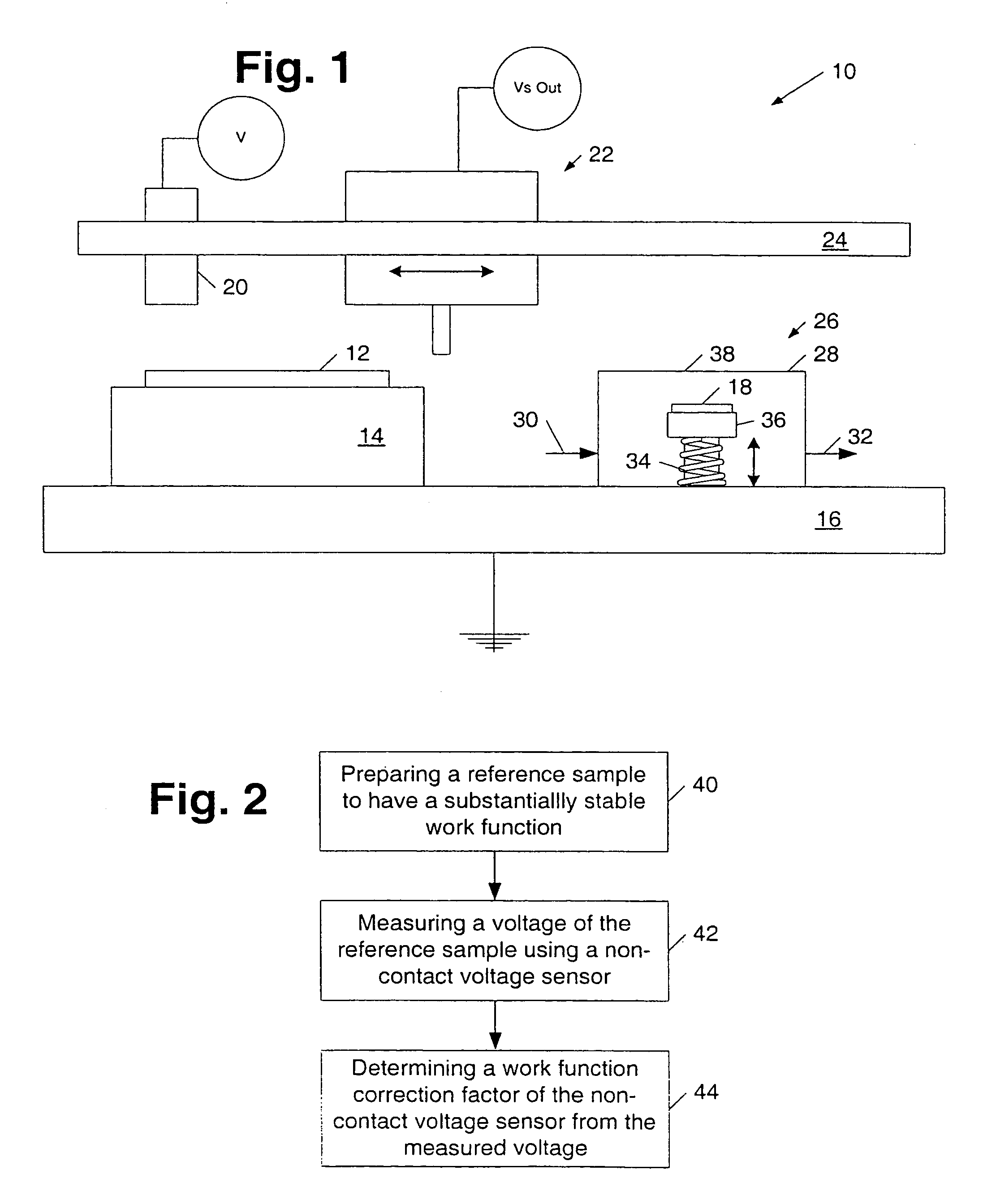
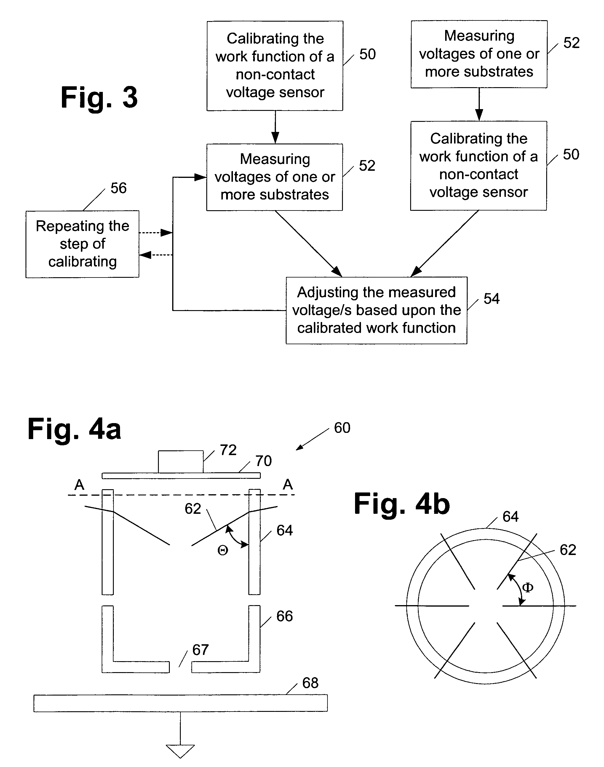
[0031]Turning now to the drawings, exemplary embodiments of systems and methods for determining properties of a wafer using non-contact electrical testing techniques as well as different configurations of corona discharge guns are illustrated in FIGS. 1–6. More specifically, FIG. 1 illustrates an exemplary embodiment of a system that employs non-contact electrical testing techniques for determining properties of a microelectronic topography, while FIGS. 2 and 3 outline methods of using such a system. In addition, FIGS. 4a–6 illustrate exemplary configurations of a device used to deposit corona charge upon a topography for electrical testing. It is noted that the systems and methods illustrated and described in reference to FIGS. 1–6 are not co-dependent and, therefore, may not necessarily be employed together.

[0032]An example of a system configured to measure charge density and voltage using non-contacting techniques is illustrated in FIG. 1. In particular, system 10 is shown config...


PUM

PropertyMeasurementUnit
anglesaaaaaaaaaa
anglesaaaaaaaaaa
widthaaaaaaaaaa

Abstract

A method and a system for calibrating the work function of a non-contact voltage sensor are provided. The method includes preparing a reference sample to have a stable work function, measuring a voltage of the sample using a non-contact voltage sensor, and determining a work function correction factor of the sensor from the measured voltage. In turn, the calibrated work function may be used to adjust voltages of substrates measured by the sensor. A corona gun which includes a first electrode and one or more conductive rods is provided. In some embodiments, the conductive rods may be angled between 0 and 90 degrees with respect to a first electrode sidewall and / or be concentrically arranged less than 90 degrees from each other. In addition or alternatively, the corona gun may be adapted to alter its length and / or include a second electrode partially inset within a space surrounded by the first electrode.

Description

PRIOR APPLICATION[0001]This application is a divisional application from prior application Ser. No. 10 / 606,066 filed Jun. 24, 2003 now U.S. Pat. No. 6,909,291.BACKGROUND OF THE INVENTION[0002]1. Field of the Invention[0003]This invention generally relates to microelectronic device manufacturing and, more specifically, to methods and systems for measuring a voltage of a microelectronic topography.[0004]2. Description of the Related Art[0005]Inaccurate analysis of one or more parameters within a microelectronic device, such as a transistor, may hinder or prohibit the function of the device, leading to a reduction in production efficiency and device quality. The characterization of thin films is especially important, since the effectiveness and reliability of thin films play an important, central role in the operation of a microelectronic device. The term “thin film” is commonly used within the microelectronic industry when referring to layers deposited upon a wafer during the fabricat...

Claims


Application Information

Patent Timeline
Patent Type & Authority Patents(United States)
IPC IPC(8): H01H47/00G01N27/00
CPCG01N27/002
Inventor XU, ZHIWEI STEVESHI, JIANOUPEI, SHIYOUMIRZAAGHAEIAN, MAHMOODRZEPIELA, JEFFREY A.
Owner KLA TENCOR TECH CORP
Why Eureka
Try Eureka