Method and apparatus for generating a device ID for stacked devices

a technology of stacked devices and unique device ids, which is applied in the field of stacking semiconductor devices, can solve the problems that the conventional method of bonding out a unique device id for each stacking device, as described above, may not be practical for future device stacking technologies

Inactive Publication Date: 2006-09-19
INTEL CORP
View PDF4 Cites 685 Cited by
  • Summary
  • Abstract
  • Description
  • Claims
  • Application Information

AI Technical Summary

Problems solved by technology

The conventional method of bonding out a unique device ID for each stacked device, as described above, may not be practical for future device stacking technologies.

Method used


Image

  • Method and apparatus for generating a device ID for stacked devices
  • Method and apparatus for generating a device ID for stacked devices
  • Method and apparatus for generating a device ID for stacked devices

Examples


Embodiment Construction

[0017]Embodiments of the present invention provide a method and apparatus for generating a unique device identifier (device ID) for each addressable integrated circuit (IC) device in a multi-die package, such as a stacked-CSP (chip scale package). Generation of a unique device ID for each stacked device is accomplished by including circuitry in each addressable device that generates a device ID based on an input device ID signal. The addressable device may then output the generated device ID to another device in the stack.

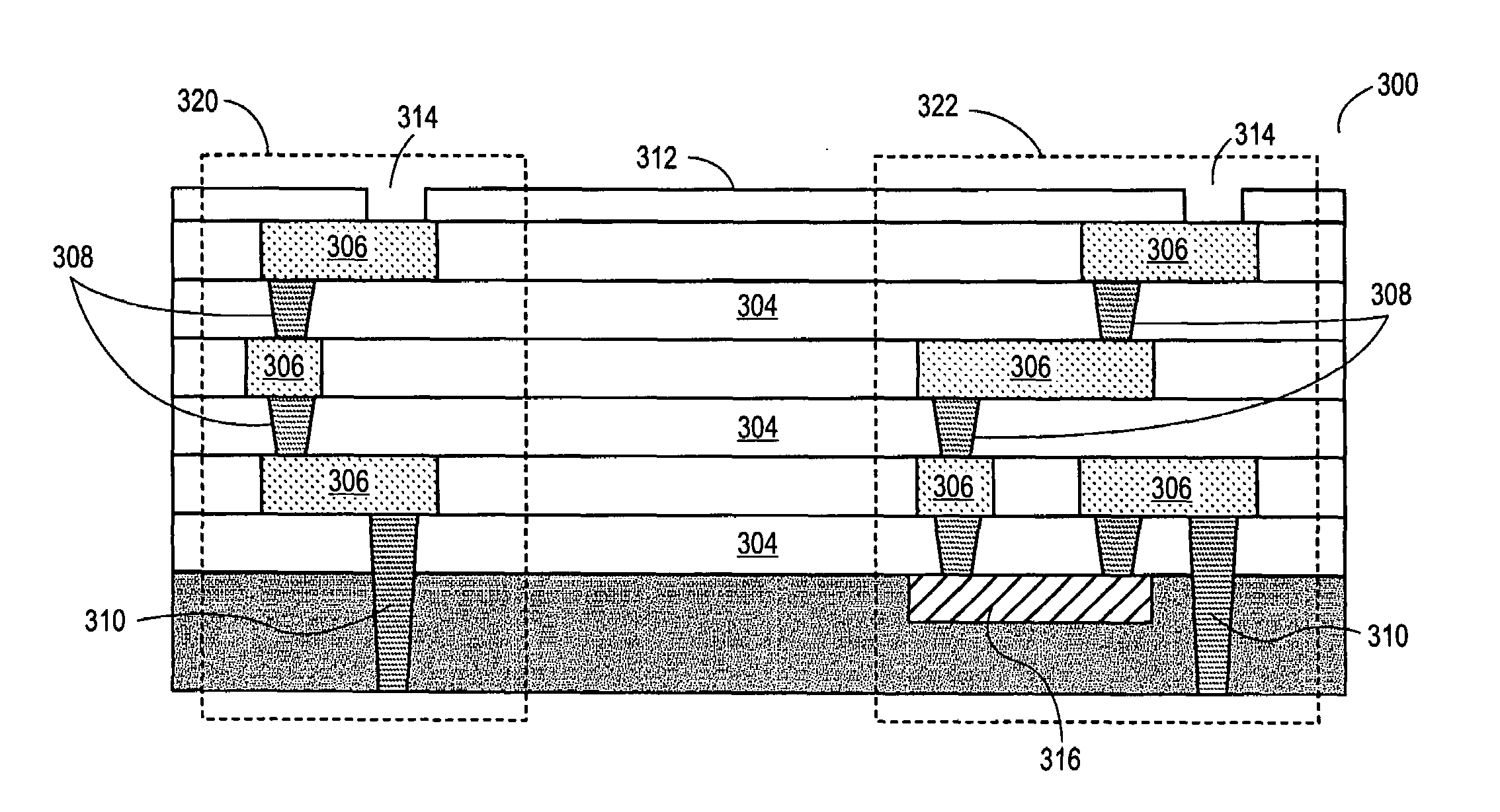
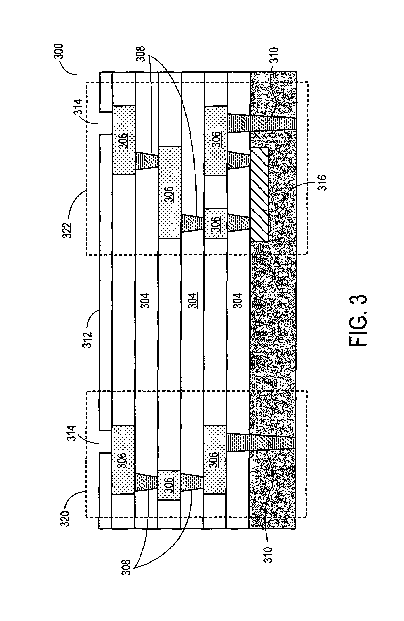
[0018]FIG. 3 illustrates a cross section of a silicon device, or die, 300 according to one embodiment of the present invention. The die 300 includes a semiconductor substrate 302 located on the bottom of the die, interlayer dielectric (ILD) layers 304, metal layers 306, vias 308 and through-silicon vias 310. Note that while bottom and top are used here to describe relative locations as indicated by the figures, one skilled in the art will appreciate that in an actu...


PUM


Abstract

A method for generating a unique device ID for each addressable device in a stack of multiple addressable devices by encoding a device ID for one device in the stack and determining a device ID for each of the other devices based on the device ID of an adjacent device in the stack.

Description

BACKGROUND OF THE INVENTION[0001]1. Field of the Invention[0002]The present invention relates to the field of stacked semiconductor devices, and more specifically to generating a unique device identifier for addressing each stacked device.[0003]2. Discussion of Related Art[0004]Addressable devices typically require some way by which each device can be addressed independently from other devices residing on the same bus. Addressable devices used in conventionally bonded stacked configurations may provide this capability by assigning each device a unique device identifier (ID). The device ID may be configured in the assembly process by bonding several device ID bondpads to power (Vcc) or ground (Vss), thereby encoding a unique device ID.[0005]FIG. 1 illustrates an exemplary approach of the current art for generating a device ID for a stacked memory device. FIG. 1 illustrates a cross-section of a package 100. The package 100 contains a package substrate 102 and two stacked memory device...

Claims


Application Information

Patent Timeline
Patent Type & Authority Patents(United States)
IPC IPC(8): G06F12/02G06F12/16
CPCG11C5/02G11C16/20H01L23/544G11C7/20H01L2223/5444H01L2223/54473H01L2225/06568H01L2224/16145H01L2224/16225H01L2224/48227H01L2924/15311H01L2225/06565H01L2224/05569H01L2224/02372H01L2224/05008H01L2224/13025H01L2224/05001H01L2224/051H01L2924/00014H01L24/05H01L2224/05599
Inventor EILERT, SEAN S.
Owner INTEL CORP
Why Eureka
Try Eureka