
Substrate inspecting method and substrate inspecting apparatus using the method

a substrate inspection and substrate technology, applied in the field of substrate inspection methods and substrate inspection apparatus, can solve problems such as trouble, affecting the accuracy of component inspection, so as to efficiently and accurately detect the component flying correspondingly

Inactive Publication Date: 2006-10-03
ORMON CORP
View PDF20 Cites 9 Cited by
  • Summary
  • Abstract
  • Description
  • Claims
  • Application Information

AI Technical Summary

Benefits of technology

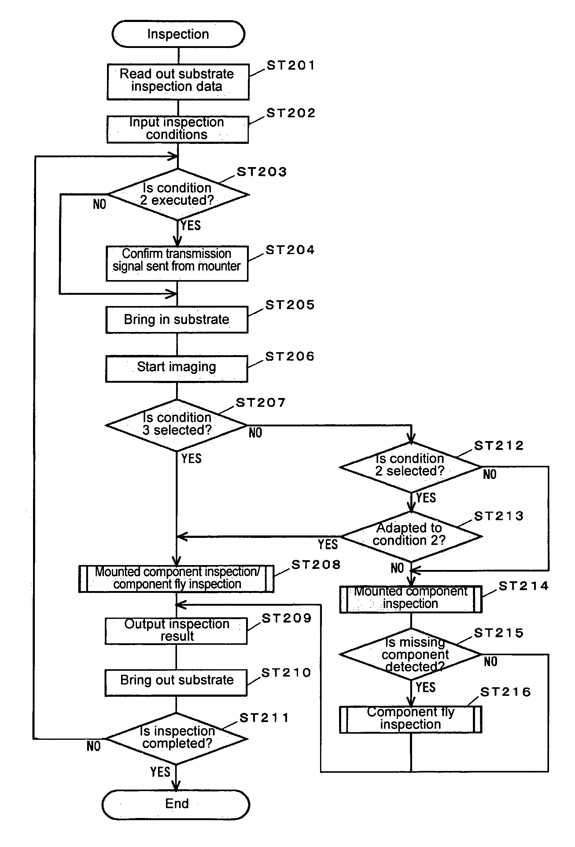
[0013]The present invention is made to solve the above problem and its object is to quickly detect this type of component fly so that a second component mounting step is not influenced by inspecting whether a component mounted in a first component mounting step is flown to a component mounting position in a second component mounting step after the first component mounting step is completed.

Problems solved by technology

Furthermore, component fly may occur also when an air pressure or attraction time for attracting a component is incorrectly set and thereby the timing for canceling the attraction of the component becomes incorrect or a component size is not fitted to the diameter of a nozzle because an incorrect component is supplied to a component supplying device.
Furthermore, when cream solder falls short because a mask clogs or a squeezee is abraded, the adhesive strength of the solder decreases.
Thus, when component fly occurs in a high-speed mounter, the flown component drops to a mounting position of the odd-shaped component, and under this state, a substrate is sent to a odd-shape mounter, the odd-shaped component is mounted on the flown component and thereby, a trouble may occur.

Method used


Image

  • Substrate inspecting method and substrate inspecting apparatus using the method
  • Substrate inspecting method and substrate inspecting apparatus using the method
  • Substrate inspecting method and substrate inspecting apparatus using the method

Examples


Embodiment Construction

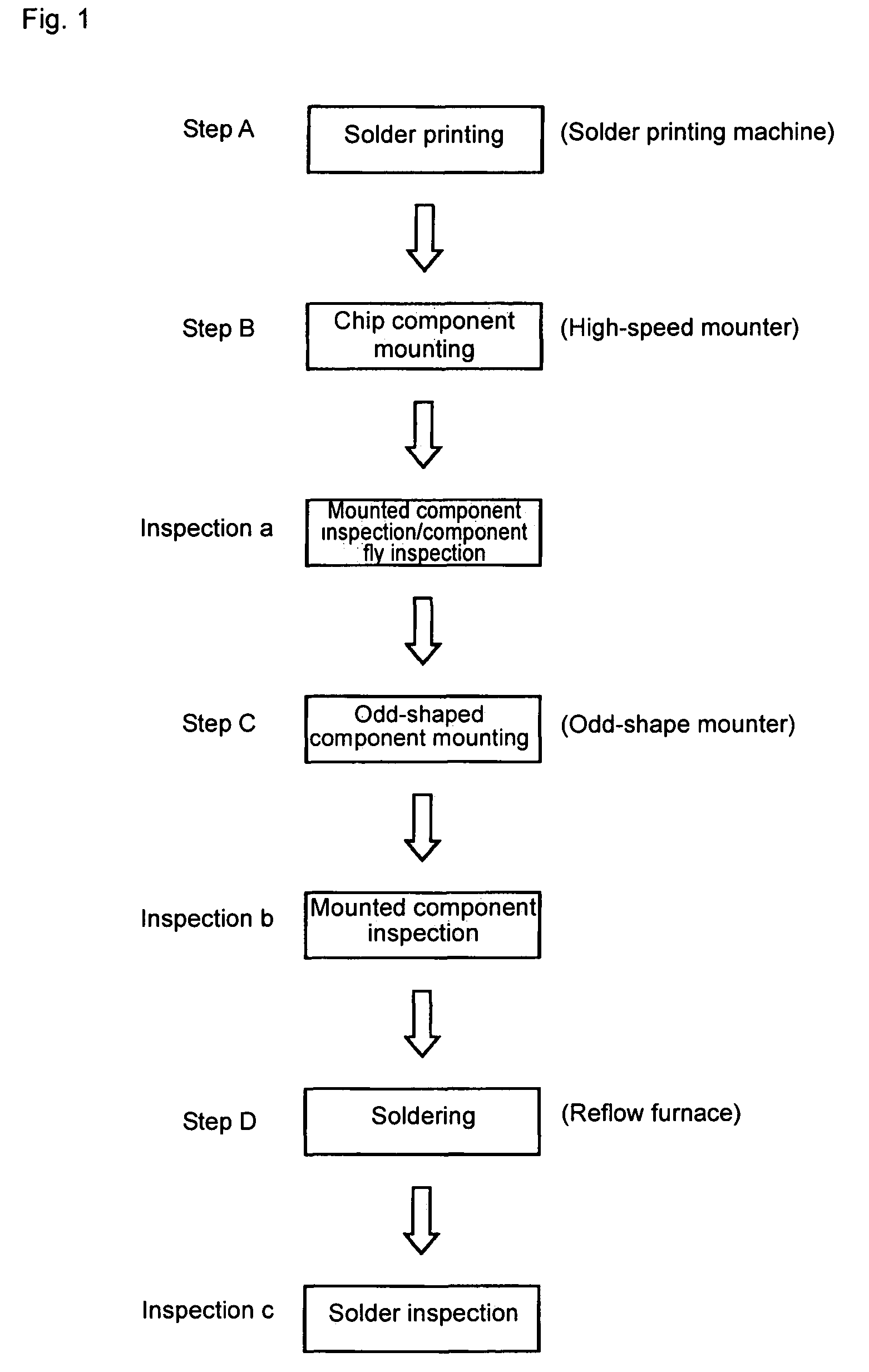
[0059]FIG. 1 shows a flow of processing in a substrate fabricating line to which the present invention is applied.

[0060]In the substrate fabricating line of this embodiment, a component mounted substrate is completed in four steps A, B, C, and D and inspections a, b, and c are executed after the steps B, C, and D.

[0061]In the first step A, cream solder is printed on a printed circuit board by a solder printing machine. In the next step B, the solder-printed substrate is supplied to a high-speed mounter to mount a chip component. Moreover, in the step C, the substrate undergoing the step B is supplied to an odd-shape mounter to mount odd-shaped components such as BGA, CSP, and IC. In the final step D, the component-mounted substrate is sent into a reflow furnace to heat the substrate and fix each component on the substrate.

[0062]Inspections a, b, and c are performed by a substrate inspecting apparatus using a computer as its main control body. The inspection a executed between the st...


PUM

PropertyMeasurementUnit
Coloraaaaaaaaaa
Sizeaaaaaaaaaa
Shapeaaaaaaaaaa

Abstract

Inspection a is executed between a step B of mounting a chip component by a high-speed mounter and a step C of mounting a odd-shaped component by a odd-shape mounter. The inspection a executes not only mounted component inspection for determining a mounted state of a chip component mounted in the preceding step but also component fly inspection for determining whether a chip component is flown to a position where a odd-shaped component is mounted in the next step C. It is possible to execute the component fly inspection in accordance with a condition corresponding to the situation of an actual spot such as a case in which it is detected that a component is missing in mounted component inspection or a case in which the replacement date of an attracting nozzle in a high-speed mounter is approaching.

Description

BACKGROUND OF THE INVENTION[0001]1. Field of the Invention[0002]The present invention relates to a technical field for inspecting a printed circuit board (hereafter referred to as “component mounting substrate” or simply referred to as “substrate”) with components mounted. Particularly, the present invention relates to an apparatus having a function for executing an inspecting method to be executed between a first component mounting step and a second component mounting step in a fabricating line in which mounting a component is executed in two separate stages and a function for executing the inspecting method.[0003]2. Description of the Prior Art[0004]A component mounting machine referred to as “mounter” has been used so far in order to automate high-density component mounting. Conventional mounters include a mounter (generally referred to as “high-speed mounter”) having a function for mounting a small component such as a chip component at a high speed and a mounter (generally refer...

Claims


Application Information

Patent Timeline
IPC IPC(8): H05K3/30G01N21/956H05K13/08G01R31/28G01R31/309
CPCG01N21/956G01R31/2813G01R31/309Y10T29/49117Y10T29/49144Y10T29/4913Y10T29/49131
Inventor MURAKAMI, KIYOSHI
Owner ORMON CORP
Learn More