Molecular logic gates

a logic gate and molecular technology, applied in the field of molecular electronics, can solve the problems of complex manufacturing of molecular-junction diodes and transistors, high cost, and high cost of soft x-rays

Inactive Publication Date: 2006-10-03
HEWLETT PACKARD DEV CO LP
View PDF3 Cites 7 Cited by
  • Summary
  • Abstract
  • Description
  • Claims
  • Application Information

AI Technical Summary

Problems solved by technology

Retooling current semiconductor-fabrication facilities to employ shorter wavelength, soft x-rays is projected to involve staggering capital expenditures.
Moreover, various physical limits of component sizes may be soon approached.
However, at nanoscale dimensions, precise fabrication of molecular-junction diode and transistors presents many challenges.

Method used


Image

  • Molecular logic gates
  • Molecular logic gates
  • Molecular logic gates

Examples


Embodiment Construction

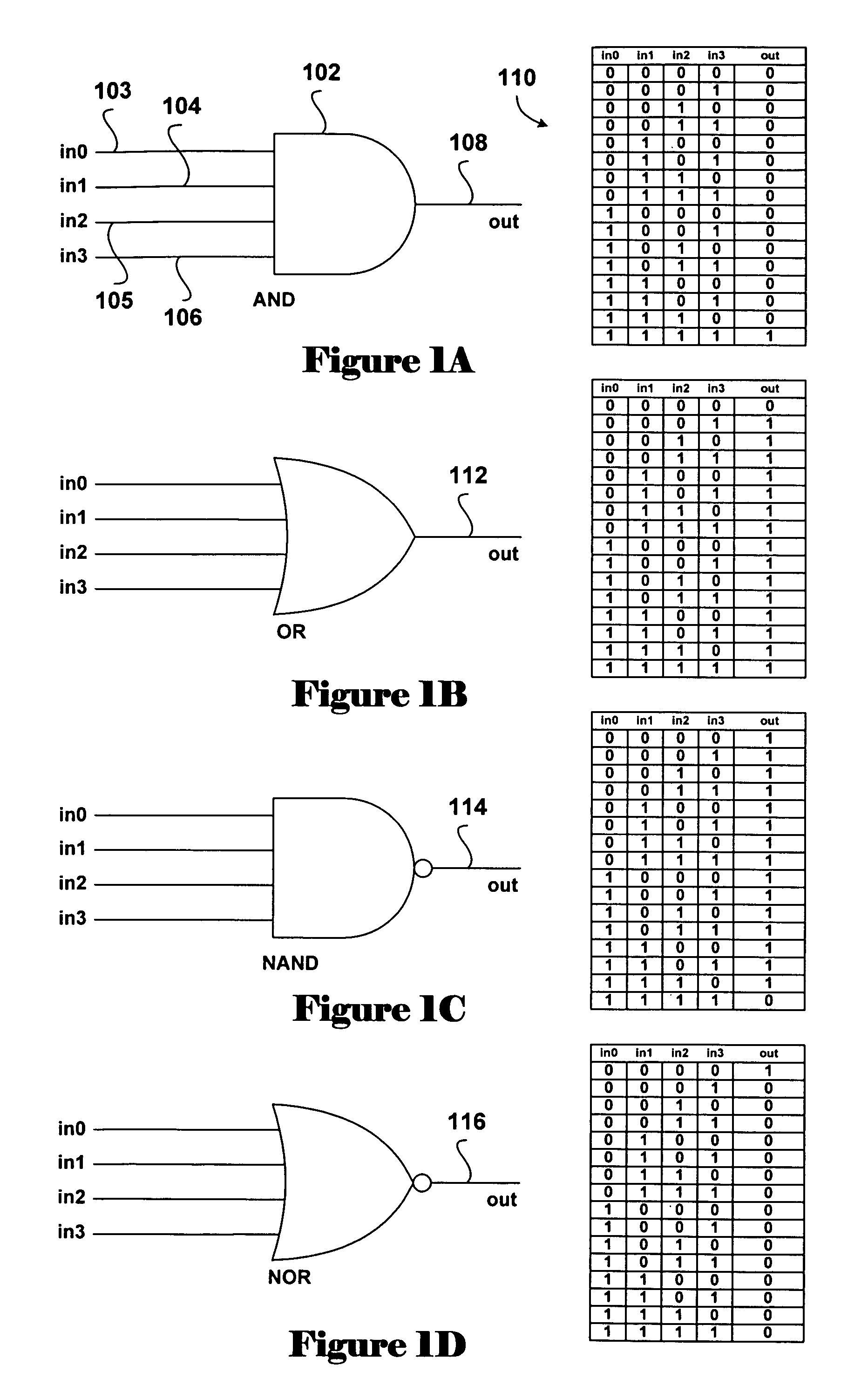
[0021]One embodiment of the present invention provides nanoscale logic gates that produce logical output signals with relatively wide voltage or current ranges that lead to readily electronically distinguishable ON and OFF logical output signals. Four specific embodiments, provided below, include AND, OR, NAND, and NOR nanoscale logic gates.

[0022]FIGS. 1A–D functionally illustrate the four, basic logic gates AND, OR, NAND and NOR. FIG. 1A shows an AND logic gate. The AND logic gate is symbolically represented as a semi-rectangularly shaped closed figure with one rounded side 102 to which a number of signal lines 103–106 are input and from which a single output signal line 108 emerges. Each input signal line 103–106 may be in a high-voltage or high-current state, normally considered a logical ON state, or a low-voltage or low-current state, normally considered a logical OFF state. These states are alternatively represented as Boolean “1” and “0,” respectively. An opposite convention ...


PUM


Abstract

Various nanoscale logic gates are disclosed. An alternating current (“AC”) source is superimposed on a direct-current (“DC”), largely resistor-based nanoscale logic circuit in order to provide distinguishable, AC current or voltage logical output signals despite potentially narrow DC-voltage or DC-current ranges produced by the resistor-based nanoscale logic circuit. AC-enhanced AND, OR, NAND, and NOR nanoscale logic gates are provided as four specific embodiments of the present invention.

Description

TECHNICAL FIELD[0001]The present invention is related to molecular electronics and, in particular, to resistor-based nanoscale logic circuits that provide easily distinguished logic output signals in response to the logical states of an arbitrary number of logical input signal lines.BACKGROUND OF THE INVENTION[0002]During the past fifty years, tremendous progress has been made in electronic technologies. Large vacuum-tube-based electronic systems were replaced with smaller, more reliable transistor-based electronics, in turn replaced with integrated-circuit technologies with ever increasing component densities and switching speeds. Currently, efforts are being made to push the standard photolithographic semiconductor-fabrication process to produce ever decreasing components sizes. One approach to decreasing component sizes is to decrease the wavelength of the light used to expose photoresist in photomasking steps. Retooling current semiconductor-fabrication facilities to employ shor...

Claims


Application Information

Patent Timeline
Patent Type & Authority Patents(United States)
IPC IPC(8): G06F17/50H03K19/02
CPCH03K19/02Y10S977/94
Inventor BAUGH, RICHARD ACHEN, YONG
Owner HEWLETT PACKARD DEV CO LP
Why Eureka
Try Eureka