Complementary metal-oxide-semiconductor field effect transistor structure having ion implant in only one of the complementary devices

a field effect transistor and metal-oxide-semiconductor technology, applied in the field of complementary metal-oxide-semiconductor field effect transistors, can solve the problems of high defect density at the oxide-semiconductor interface, rendering the devices essentially useless, and successfully fabricated channel emosfets

Active Publication Date: 2006-10-10
NORTH STAR INNOVATIONS
View PDF8 Cites 120 Cited by
  • Summary
  • Abstract
  • Description
  • Claims
  • Application Information

AI Technical Summary

Benefits of technology

[0005]In accordance with one practical embodiment, a complementary metal-oxide-semiconductor FET structure uses ion implants for only one type of device (either the n-channel or the p-channel device). Using this structure, sheet resistivity of 100 Ohm / square and below is achievable within a practical thermal budget, which allows for high performance devices, particularly at short gate lengths.

Problems solved by technology

However, only p-channel EMOSFETs have been successfully fabricated on the compound semiconductor GaAs in the past.
For n-channel EMOSFETs on GaAs, the implant activation temperature for donors of >700° C. is incompatible with Ga2O3—GaAs interface stability.
However, the subsequent gate oxide deposition is inevitably conducted on an exposed semiconductor surface, which leads to a high defect density at the oxide-semiconductor interface.
The high defect density only allows the fabrication of devices with about 1% of anticipated performance, rendering the devices essentially useless.

Method used


Image

  • Complementary metal-oxide-semiconductor field effect transistor structure having ion implant in only one of the complementary devices
  • Complementary metal-oxide-semiconductor field effect transistor structure having ion implant in only one of the complementary devices

Examples


Embodiment Construction

[0010]The following detailed description is merely exemplary in nature and is not intended to limit the invention or the application and uses of the invention. Furthermore, there is no intention to be bound by any expressed or implied theory presented in the preceding technical field, background, brief summary or the following detailed description.

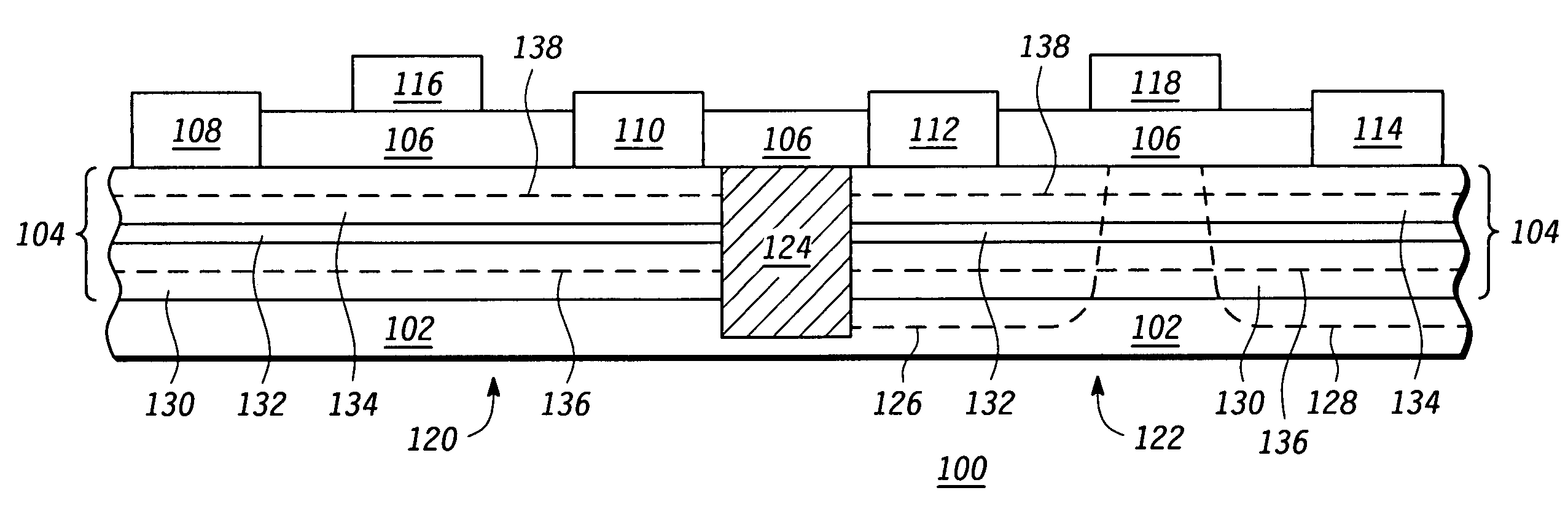
[0011]FIG. 1 is a cross sectional view of a complementary metal-oxide-compound semiconductor field effect transistor structure 100 configured in accordance with an example embodiment of the invention. Transistor structure 100 generally includes a semiconductor substrate 102, an epitaxial layer structure 104 formed on semiconductor substrate 102, a gate oxide layer 106, Ohmic contacts (identified by reference numbers 108, 110, 112, and 114), and gate electrodes (identified by reference numbers 116 and 118). In one embodiment of the invention, semiconductor substrate 102 is a compound semiconductor substrate. Transistor structure 100 include...


PUM


Abstract

A complementary metal-oxide-semiconductor field effect transistor structure includes ion implants in only one of the two complementary devices. The transistor structure generally includes a compound semiconductor substrate and an epitaxial layer structure that includes one or more donor layers that establish a conductivity type for the epitaxial layer structure. The ion implants function to “invert” or “reverse” the conductivity type of the epitaxial layer structure in one of the complementary devices. In the example embodiment, p-type acceptor implants are utilized in the p-channel device, while the n-channel device remains implant-free.

Description

TECHNICAL FIELD[0001]The present invention generally relates to semiconductor devices and, more particularly, to complementary metal-oxide-semiconductor field effect transistors.BACKGROUND[0002]The prior art is replete with different complementary metal-oxide-semiconductor field effect transistor (MOSFET) technologies. For example, enhancement mode metal-oxide-semiconductor field effect transistors (EMOSFETs) on compound semiconductors can employ standard-refractory metal gates with a metal work function of about 4.6 eV, an undoped channel to provide enhancement mode operation (positive and negative threshold voltage for n-channel and p-channel devices, respectively), and self-aligned ion implants to form low resistivity source and drain extensions and Ohmic contact regions. However, only p-channel EMOSFETs have been successfully fabricated on the compound semiconductor GaAs in the past. For n-channel EMOSFETs on GaAs, the implant activation temperature for donors of >700° C. is ...

Claims


Application Information

Patent Timeline
Patent Type & Authority Patents(United States)
IPC IPC(8): H01L21/00
CPCH01L27/0605H01L29/51H01L21/823814H01L27/092
Inventor PASSLACK, MATTHIAS
Owner NORTH STAR INNOVATIONS
Why Eureka
Try Eureka