

Method for aligning wafer
a wafer alignment and wafer technology, applied in the direction of photomechanical equipment, coupling device connections, instruments, etc., can solve the problems of deteriorating overlay accuracy, inability to detect alignment signals by wafer alignment sensors, severe deformation of overlay accuracy of lithography processes, etc., to improve overlay accuracy for the underlying layer
- Summary
- Abstract
- Description
- Claims
- Application Information
AI Technical Summary
Benefits of technology
Problems solved by technology
Method used
Image

Examples
Embodiment Construction
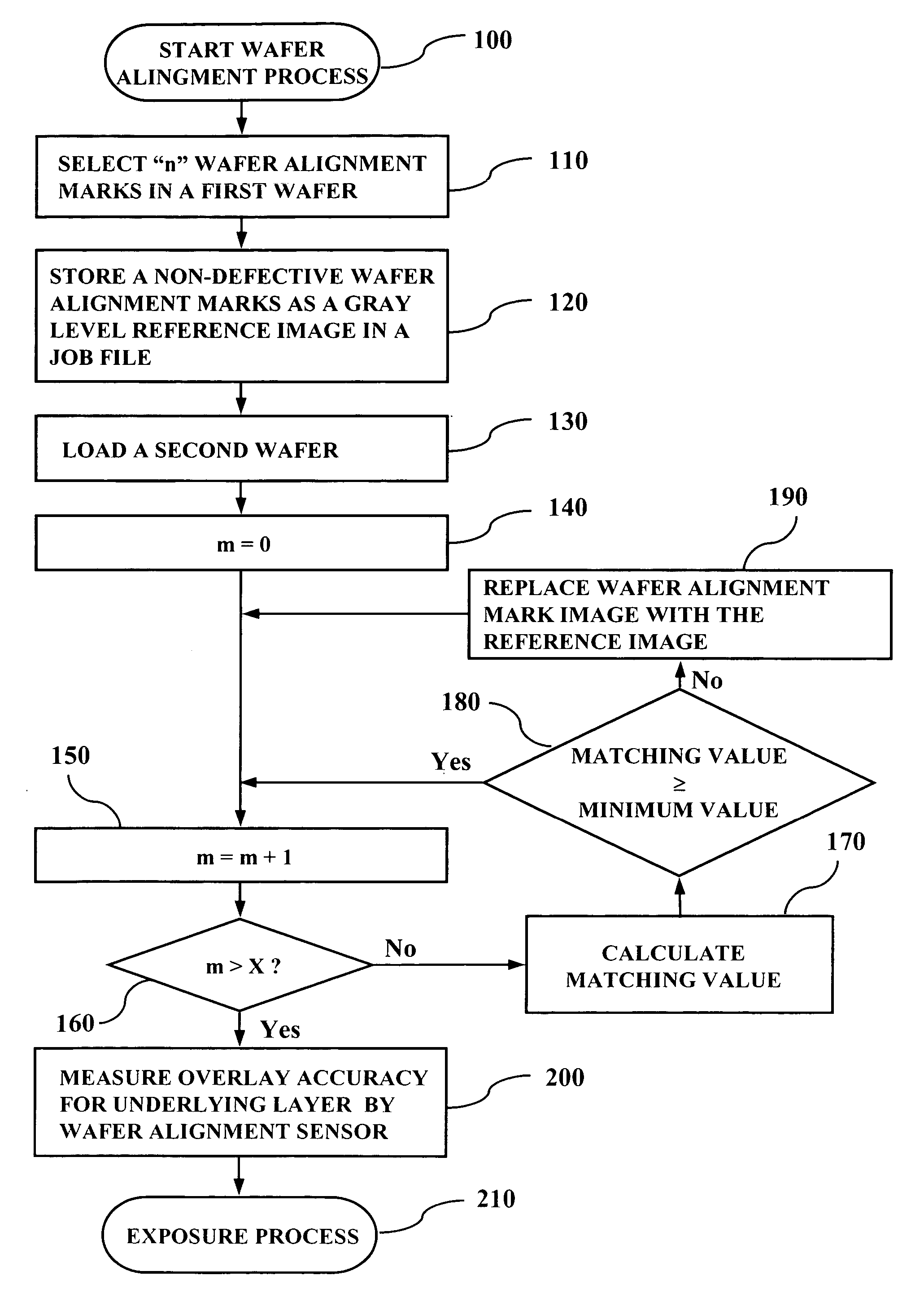
[0019]A method for aligning wafer in accordance with an embodiment of the present invention will now be described in detail with reference to the accompanying drawings. Wherever possible, the same reference numerals will be used throughout the drawings to refer to the same or like parts.
[0020]FIG. 1 depicts an image-processing wafer alignment algorithm using a comparison and replacement method with a reference image.
[0021]Step 100 through step 210 will be described referring to FIG. 1.
[0022][Step 100] and [Step 110]
[0023]The method for alignment of a wafer in accordance with the present invention starts at step 100 where a sample wafer is loaded and aligned in an exposure apparatus.
[0024]N wafer alignment marks in a job file are selected from the first wafer, where “n” is a natural number. Here, the selected alignment marks are chosen from the entire die in the wafer.
[0025][Step 120]
[0026]A non-defective wafer alignment mark is selected among the selected wafer alignment marks of th...
PUM
| Property | Measurement | Unit |
|---|---|---|
| size | aaaaa | aaaaa |
| distance | aaaaa | aaaaa |
Abstract
Description
Claims
Application Information