

Overlay precision correction method
A technology of overlay accuracy and overlay error, which is applied in microlithography exposure equipment, optics, instruments, etc., and can solve the problem of large overlay error
- Summary
- Abstract
- Description
- Claims
- Application Information
AI Technical Summary
Problems solved by technology
Method used
Image

Examples
Embodiment Construction
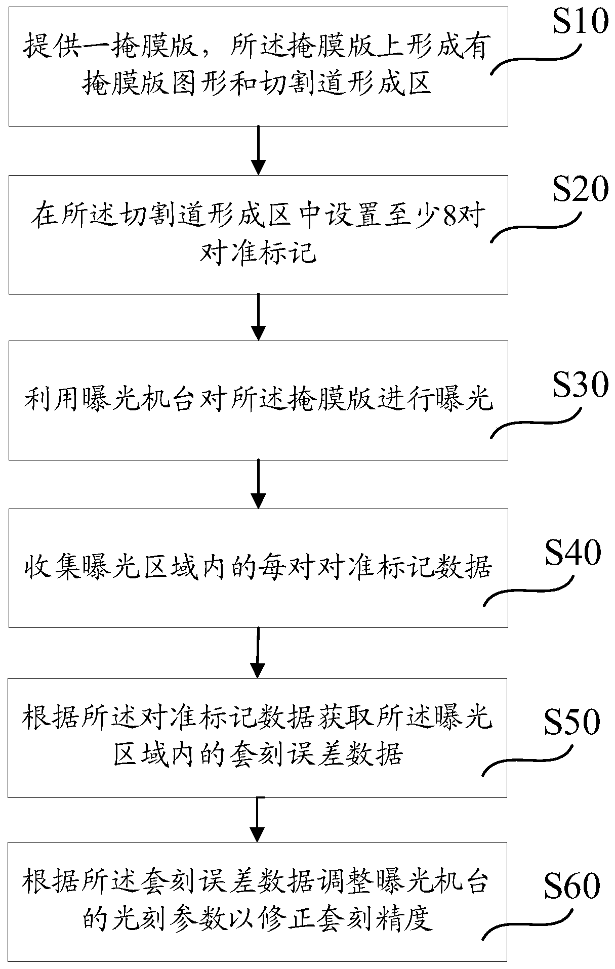
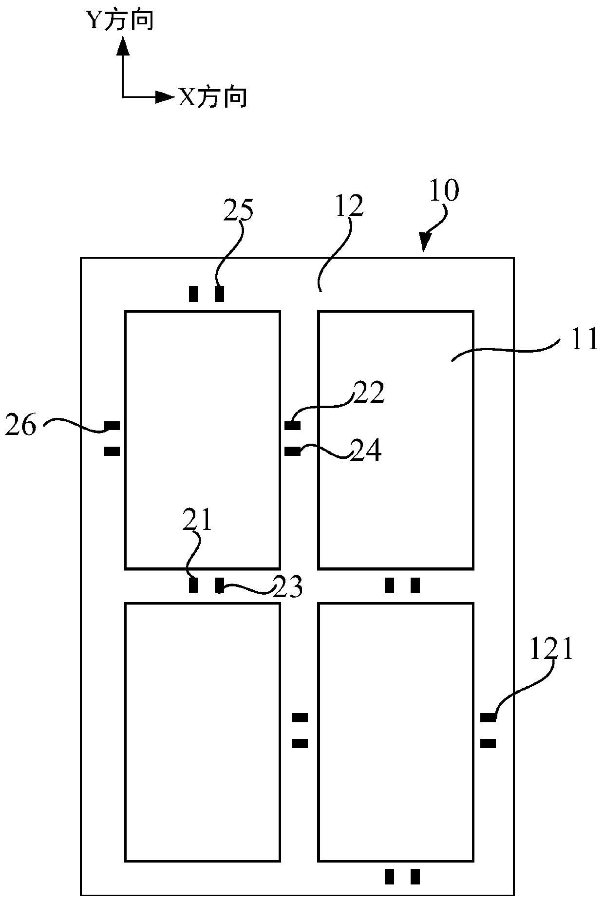
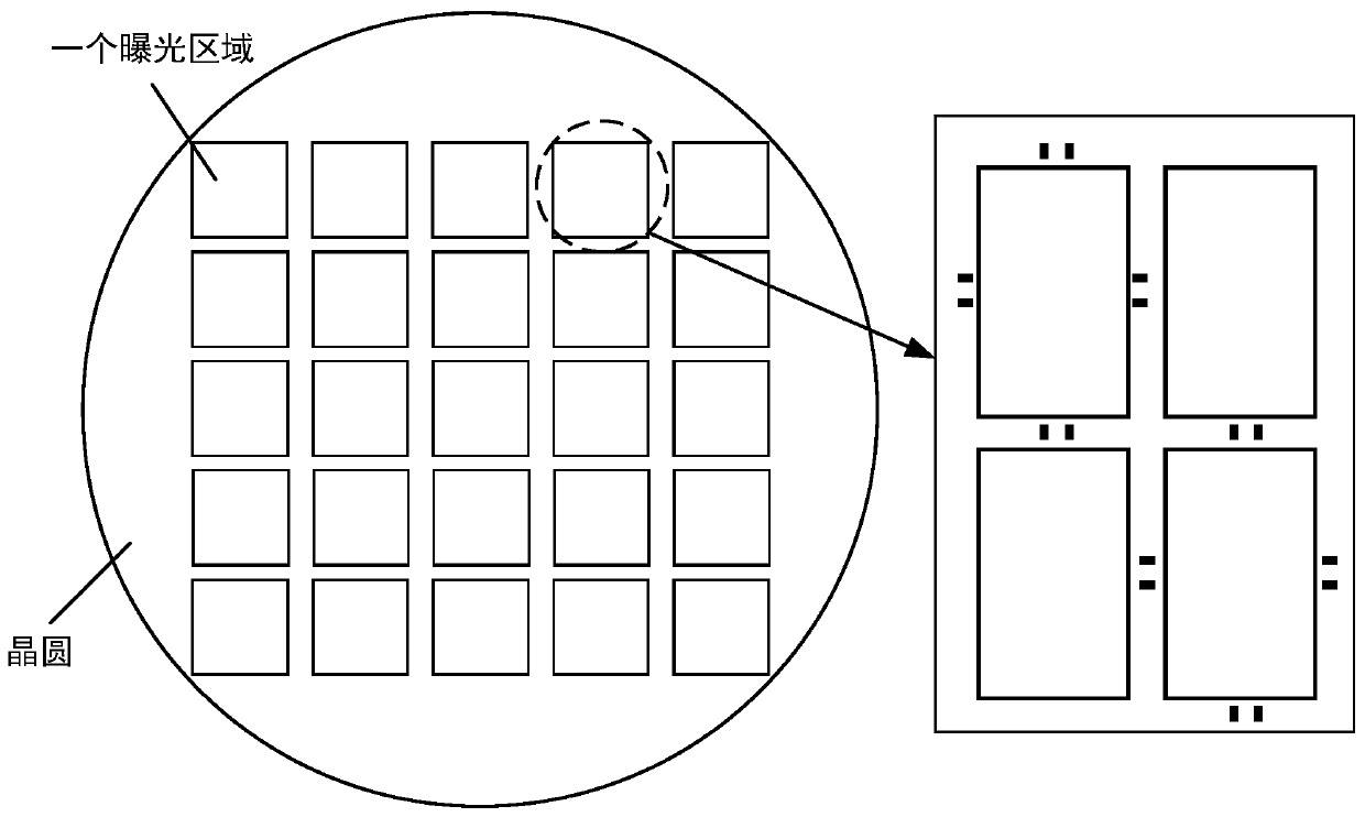
[0037] The overlay precision correction method proposed by the present invention will be further described in detail below in conjunction with the accompanying drawings and specific embodiments. Advantages and features of the present invention will be apparent from the following description and claims. It should be noted that all the drawings are in a very simplified form and use imprecise scales, and are only used to facilitate and clearly assist the purpose of illustrating the embodiments of the present invention. In addition, the structures shown in the drawings are often a part of the actual structure. In particular, each drawing needs to display different emphases, and sometimes uses different scales.
[0038] The simple model in the current prior art is a linear correction model, which usually uses six parameters: translation parameters in the X and Y directions; contraction or enlargement parameters in the X and Y directions; rotation parameters; and diagonal distortio...
PUM
 Abstract
Description
Claims
Application Information