A method for reducing the deformation of silicon wafer caused by adsorption of photolithography workpiece table

A technology of workpiece table and silicon wafer, which is applied in the field of photolithography technology, can solve the problems that cannot be directly eliminated, such as the difference of overlay precision vector, and achieve the effect of reducing overlay error, improving product yield and reducing error

Active Publication Date: 2018-10-16
SHANGHAI INTEGRATED CIRCUIT RES & DEV CENT
View PDF4 Cites 0 Cited by
  • Summary
  • Abstract
  • Description
  • Claims
  • Application Information

AI Technical Summary

Problems solved by technology

[0003] During the process, the silicon wafer is adsorbed on the workpiece table. Since the workbench and the lower surface of the silicon wafer in contact with the workbench are randomly distributed with uneven areas, under the same adsorption force, different parts of the silicon wafer will produce The adsorption deformation is different, which brings about the warping of the upper surface of the silicon wafer due to the adsorption deformation, which causes some deformation points to be unable to be within the focusing range of the workpiece table through the focusing and leveling system , resulting in the vector difference of the overlay accuracy in the X and Y directions of the workpiece table plane
And the distribution of these vector differences is also random, which cannot be directly eliminated by a preset method
The impact of these differences on overlay accuracy can only be minimized by means of detection-correction

Method used


Image

  • A method for reducing the deformation of silicon wafer caused by adsorption of photolithography workpiece table
  • A method for reducing the deformation of silicon wafer caused by adsorption of photolithography workpiece table
  • A method for reducing the deformation of silicon wafer caused by adsorption of photolithography workpiece table

Examples


Embodiment Construction

[0025] The specific embodiment of the present invention will be further described in detail below in conjunction with the accompanying drawings.

[0026] It should be noted that, in the following specific embodiments, when describing the embodiments of the present invention in detail, in order to clearly show the structure of the present invention for the convenience of description, the structures in the drawings are not drawn according to the general scale, and are drawn Partial magnification, deformation and simplification are included, therefore, it should be avoided to be interpreted as a limitation of the present invention.

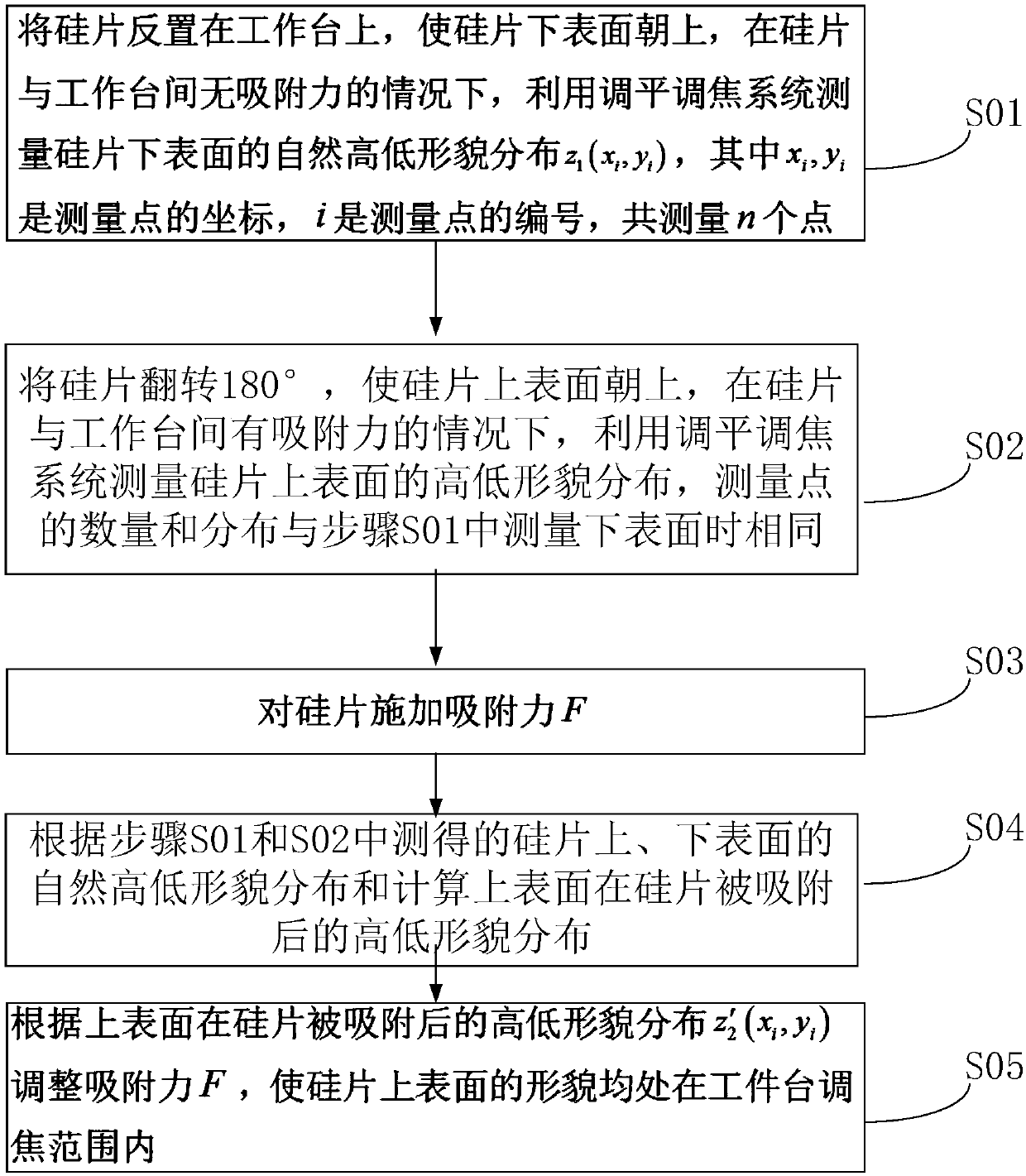
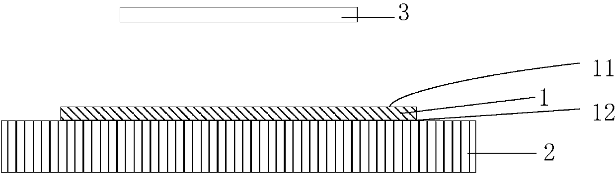
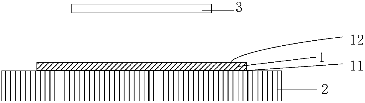
[0027] In the following specific embodiments of the present invention, please refer to figure 1 , figure 1 It is a schematic flow chart of a method for reducing the deformation of silicon wafers caused by the adsorption of photolithographic worktables in the present invention. Such as figure 1 As shown, a method disclosed in the present invention ...


PUM


Abstract

The invention discloses a method for reducing silicon wafer deformation caused by photoetching workpiece platform adsorption. The method comprises the following steps: obtaining high and low morphology distribution of the lower surface of a silicon wafer when an adsorption force does not exist through measurement, applying an adsorption force to a photoetching workpiece platform, simulating and calculating the high and low morphology distribution of the upper surface of the silicon wafer, and inspecting the distribution to ensure that the high and low morphology of the upper surface of the silicon wafer is positioned within the focusing range of the workpiece platform after adsorption and form an ideal plane as much as possible. By the method, the silicon wafer deformation caused by photoetching workpiece platform adsorption is reduced, so that the overlay error on the workpiece platform plane caused by the adsorption force is reduced and the yield of products is increased.

Description

technical field [0001] The present invention relates to a photolithography process method, in particular to a photolithography process method for supplementing the overlay accuracy of a photolithography machine. Background technique [0002] With the development of photolithography technology, higher and higher requirements are put forward for overlay precision. For ideal photolithography, the flatter the silicon wafer, the larger the process production window can be obtained, thereby improving the overlay accuracy to meet the increasingly higher process requirements such as line width critical dimensions. However, a perfect absolutely flat silicon wafer does not exist. During the production process, the process equipment deals with uneven silicon wafers. The unevenness of the silicon wafer is mainly caused by several reasons: first, the manufacturing process of the silicon wafer itself; second, the defects caused by the silicon wafer after the previous process steps, inclu...

Claims


Application Information

Patent Timeline
Patent Type & Authority Patents(China)
IPC IPC(8): G03F7/20
CPCG03F7/70716G03F7/70725G03F7/7085
Inventor 姚树歆李铭
Owner SHANGHAI INTEGRATED CIRCUIT RES & DEV CENT
Why Eureka
Try Eureka