Dual trench alternating phase shift mask fabrication

a phase shift mask and dual trench technology, applied in the field of semiconductor device fabrication, can solve the problems of large lithographic process burden, difficult resolution of anything smaller than a wavelength, and sub-wavelength lithography, and achieve the effects of reducing the overlay error, and reducing the cost of induced anti-reflective layer loss

Inactive Publication Date: 2007-08-16
TAIWAN SEMICON MFG CO LTD
View PDF6 Cites 0 Cited by
  • Summary
  • Abstract
  • Description
  • Claims
  • Application Information

AI Technical Summary

Benefits of technology

[0017] The invention provides for advantages not found within the prior art. E-beam writing is significantly reduced in fabricating a dual-trench alternating PSM, as compared to the prior art, by instead usinq backside ultraviolet exposure. This significantly decreased overlay error, which means that induced anti-reflective layer loss is also significantly reduced. Backside ultraviolet exposure can be used because of the presence of the mask layer, which may be molybdenum silicon oxide (MoSiO), which prevents such exposure from affecting the chromium layer. The reduction in use of e-beam writing also means that the invention generates a dual-trench alternating PSM in a less costly and / or less time-consuming manner as compared to the prior art. Other advantages, embodiments, and aspects of the invention will become apparent by reading the detailed description that follows, and by referencing the attached drawings.

Problems solved by technology

Sub-wavelength lithography, however, places large burdens on lithographic processes.
Resolution of anything smaller than a wavelength is generally quite difficult.
Pattern fidelity can deteriorate in sub-wavelength lithography.
For example, as two mask patterns get closer together, diffraction problems occur.
Any light that spills over into the dark region from the two edges that are out of phase will destructively interfere.
Overlay errors can error between successive exposures of the photoresist, such as between successive e-beam writings.
These overlay errors induce anti-reflective layer loss around the etched regions, which can be difficult to discover during inspection.
Because photoresist is exposed for a total of eight times, there are eight such successive e-beam writings, and the potential for overlay error inducing anti-reflective layer loss is great.
Furthermore, e-beam writing in particular can be a time-consuming and / or costly process, such that fabricating the PSM 300 will be a lengthy and / or costly process since e-beam writing is used eight times.
Furthermore, such minimization will decrease the time and / or the cost in fabricating dual-trench alternating PSM's.

Method used


Image

  • Dual trench alternating phase shift mask fabrication
  • Dual trench alternating phase shift mask fabrication
  • Dual trench alternating phase shift mask fabrication

Examples


Embodiment Construction

[0024] In the following detailed description of exemplary embodiments of the invention, reference is made to the accompanying drawings that form a part hereof, and in which is shown by way of illustration specific exemplary embodiments in which the invention may be practiced. These embodiments are described in sufficient detail to enable those skilled in the art to practice the invention. Other embodiments may be utilized, and logical, mechanical, and other changes may be made without departing from the spirit or scope of the present invention. The following detailed description is, therefore, not to be taken in a limiting sense, and the scope of the present invention is defined only by the appended claims.

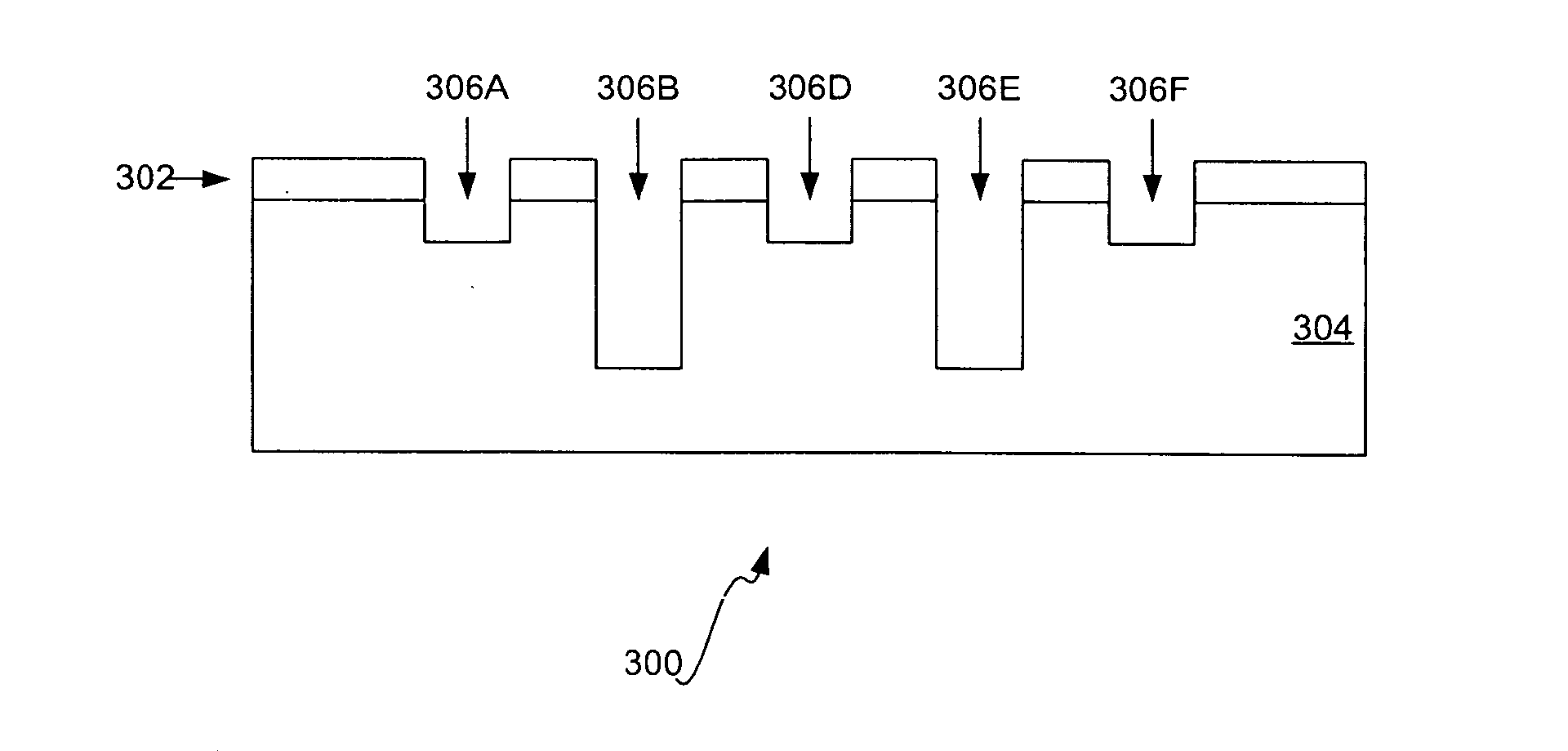
[0025]FIGS. 5A and 5B show a method 500 to construct a dual-trench alternating phase shift mask (PSM) according to an embodiment of the invention. In FIG. 5A, a photoresist layer over a chromium layer is first exposed according to a semiconductor design (502), such as by e-beam w...


PUM


Abstract

Fabricating a dual-trench alternating phase shift mask (PSM) is disclosed. A chromium layer over a mask layer, which is over a quartz layer, of the PSM is patterned according to a semiconductor design. The mask layer is dry etched according to deep trenches of a PSM design. The quartz layer is dry etched a first number of times through a first photoresist layer applied over the chromium layer and patterned according to the deep trenches of the PSM design by using backside ultraviolet exposure. The mask layer is dry etched again, according to shallow trenches of the PSM design. The quartz layer is dry etched a second number of times through a second photoresist layer applied over the chromium layer and patterned according to the shallow trenches of the PSM design by using backside ultraviolet exposure.

Description

FIELD OF THE INVENTION [0001] This invention relates generally to semiconductor device fabrication, and more particularly to the use of phase shift masks (PSM's) in conjunction with such fabrication. BACKGROUND OF THE INVENTION [0002] Since the invention of the integrated circuit (IC), semiconductor chip features have become exponentially smaller and the number of transistors per device exponentially larger. Advanced IC's with hundreds of millions of transistors at feature sizes of 0.25 micron, 0.18 micron, and less are becoming routine. Improvement in overlay tolerances in photolithography, and the introduction of new light sources with progressively shorter wavelengths, have allowed optical steppers to significantly reduce the resolution limit for semiconductor fabrication far beyond one micron. To continue to make chip features smaller, and increase the transistor density of semiconductor devices, IC's have begun to be manufactured that have features smaller than the lithographic...

Claims


Application Information

Patent Timeline
Patent Type & Authority Applications(United States)
IPC IPC(8): H01L21/461H01L21/302H01L29/76
CPCG03F1/30
Inventor TZU, SAN-DEYEN, MING-SHUOCHANA, CHUNG-HSING
Owner TAIWAN SEMICON MFG CO LTD
Why Eureka
Try Eureka