Method for improving warping degree of silicon wafer and increasing alignment precision

A technology of overlay accuracy and warpage, which is applied in the data processing of the layout, improves the warpage of silicon wafers, and improves the overlay accuracy. Stress, effect of changing warpage

Active Publication Date: 2019-05-03
SHANGHAI HUALI MICROELECTRONICS CORP
View PDF6 Cites 8 Cited by
  • Summary
  • Abstract
  • Description
  • Claims
  • Application Information

AI Technical Summary

Problems solved by technology

Laser annealing has also been introduced into the manufacturing process of integrated circuits for ultra-shallow, high activation and low resistance, but it will have a negative impact on the stress of the wafer and the overlay accuracy of lithography

Method used


Image

  • Method for improving warping degree of silicon wafer and increasing alignment precision
  • Method for improving warping degree of silicon wafer and increasing alignment precision
  • Method for improving warping degree of silicon wafer and increasing alignment precision

Examples


Embodiment Construction

[0055] The following will clearly and completely describe the technical solutions in the embodiments of the present invention with reference to the accompanying drawings in the embodiments of the present invention. Obviously, the described embodiments are only some of the embodiments of the present invention, not all of them. Based on the embodiments of the present invention, all other embodiments obtained by persons of ordinary skill in the art without creative efforts fall within the protection scope of the present invention.

[0056] It should be noted that, in the case of no conflict, the embodiments of the present invention and the features in the embodiments can be combined with each other.

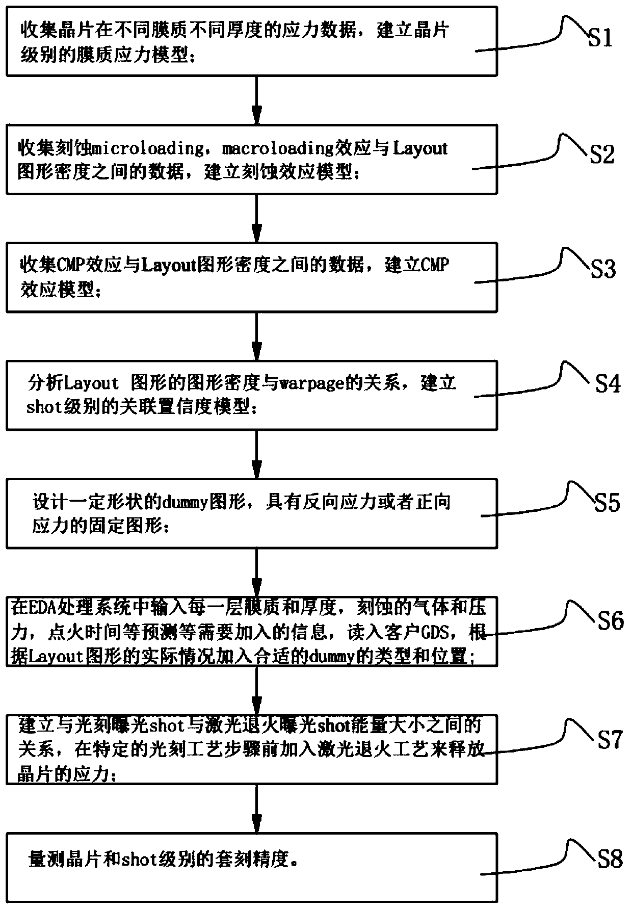
[0057] As a preferred embodiment, such as Figure 1-3 As shown, a method for improving the warpage of silicon wafers and improving the overlay accuracy, the film quality stress model used to obtain the stress data of silicon wafers, the relationship between the load effect of silico...


PUM

PropertyMeasurementUnit
Overlap degreeaaaaaaaaaa

Abstract

The invention discloses a method for improving the warping degree of a silicon wafer and increasing the alignment precision, and the method comprises the following steps: changing the layout and the graph density through an added specific auxiliary design graph so as to provide reverse stress or forward stress on a wafer; then, keeping an auxiliary design pattern in a subsequent chemical mechanical polishing process or an etching process, so as to achieve the purpose of changing the warping degree of the wafer; meanwhile, introducing a laser annealing process before a photoetching process stepin order to ensure the release of the internal stress of the whole wafer Shot, and cooperatively adjusting the energy of laser annealing and the size of Shot to achieve the purposes of releasing thewafer stress at a specific position through cooperating with the size of the photoetching exposure Shot.

Description

technical field [0001] The invention relates to the field of integrated circuit manufacturing, relates to a layout data processing method, in particular to a method for improving the warping degree of a silicon chip and improving the engraving precision. Background technique [0002] With the continuous reduction of lithographic feature size, the requirements for overlay accuracy and critical dimension uniformity of lithography machines are also increasing. The manufacture of integrated circuits usually includes dozens of photolithography processes. In order to ensure the corresponding relationship of each level, it is necessary to require an overlay accuracy that matches the photolithography feature size. The difference between the exposure pattern and the actual position, that is, the pattern position offset, is an important factor affecting the overlay accuracy of the lithography machine, and is also an important factor affecting the device. [0003] The overlay accuracy...

Claims


Application Information

Patent Timeline
Patent Type & Authority Applications(China)
IPC IPC(8): G03F7/20
Inventor 孟鸿林姜立维陈翰张辰明
Owner SHANGHAI HUALI MICROELECTRONICS CORP
Why Eureka
Try Eureka