Semiconductor package

a technology of semiconductors and packaging, applied in the direction of printed circuits, sustainable manufacturing/processing, final product manufacturing, etc., can solve the problems of effusion, difficult control of injection of underfill material into the space, and dissolution, so as to reduce the effusion of adhesive materials, reduce the amount of material used, and save processing steps and processing time

Active Publication Date: 2006-10-24
ADVANCED SEMICON ENG INC
View PDF2 Cites 0 Cited by
  • Summary
  • Abstract
  • Description
  • Claims
  • Application Information

AI Technical Summary

Benefits of technology

[0006]Accordingly, at least one objective of the present invention is to provide a semiconductor package structure capable of rectifying the underfill material injection problems in a conventional manufacturing method.
[0008]Because the connection structure runs along the periphery of the bottom surface of the semiconductor device, the connection structure not only stabilizes and provides additional support to the package but also reduces stresses between the semiconductor device and the substrate. Ultimately, the semiconductor package can be subjected to a higher stress without delamination.
[0010]Furthermore, a suitable adhesive (for example, a soft plastic material) can be selected to form a connection structure having a desired degree of flexibility so that the connection structure may serve as a buffer to protect the semiconductor package against shock.
[0012]According to one embodiment of the present invention, the coating of adhesive on the bottom surface of the semiconductor device can be carried out before the semiconductor device is flip-chip bonded to the substrate. In essence, flip-chip bonding comprises performing a reflow process at a high temperature to melt a plurality of solder balls and then cool down the solder balls to form connections between the semiconductor package and the substrate. In the present embodiment, an adhesive material having a curing temperature close to the melting point of the solder balls can be selected so that the connection structure is formed after the reflow process. After coating the adhesive material on the bottom surface of the semiconductor device, the high temperature reflow process can be used to bond the semiconductor package and the substrate together and cure the adhesive at the same time. In other words, there is considerable saving in processing step and processing time.
[0013]Since the present invention demands the coating of adhesive along at least a portion of the bottom periphery of the semiconductor device instead of injecting underfill material into the gap between the semiconductor device and the substrate, less material can be used. Thus, the fabricating method of the present invention not only reduces the effusion adhesive material but also speeds the production of the connective structure.

Problems solved by technology

Moreover, the heat-produced moisture or pollutants are still enclosed by the underfill layer 106 under thermal vaporization, incapable of dissipating away.
In general, the gap between the semiconductor device 102 and the substrate 104 is relatively small so that it is very difficult to have a controlled injection of underfill material into the space, and the problem of effusion occurs often.

Method used


Image

  • Semiconductor package
  • Semiconductor package
  • Semiconductor package

Examples


Embodiment Construction

[0022]Reference will now be made in detail to the present preferred embodiments of the invention, examples of which are illustrated in the accompanying drawings. Wherever possible, the same reference numbers are used in the drawings and the description to refer to the same or like parts.

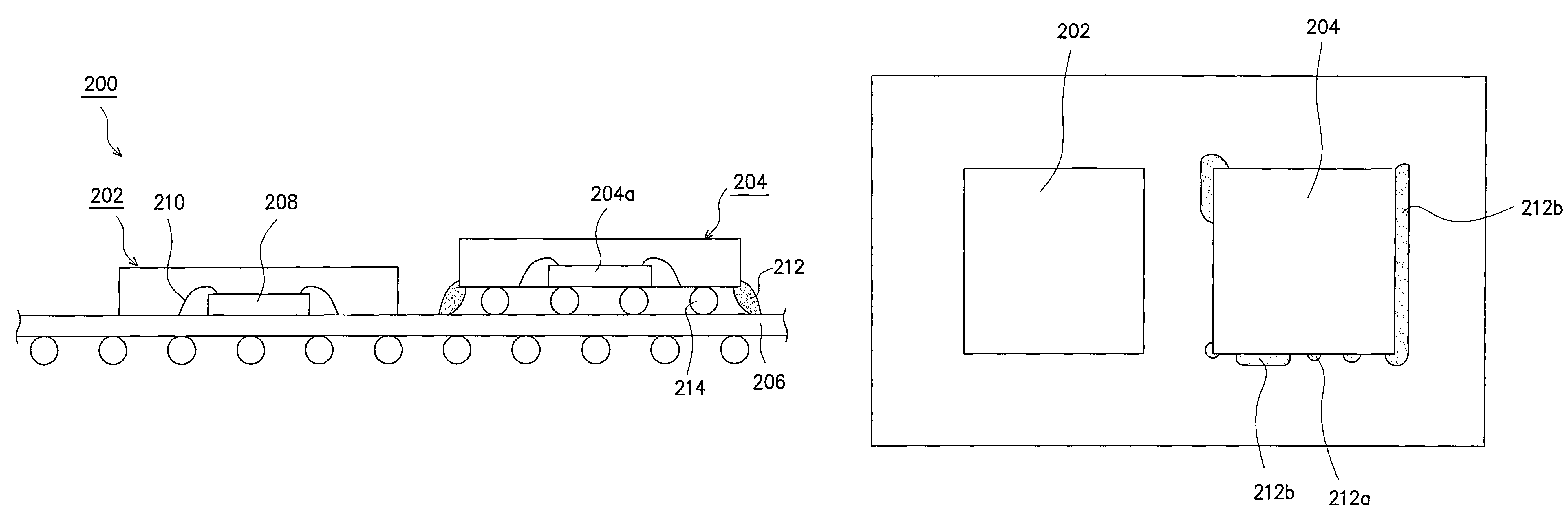
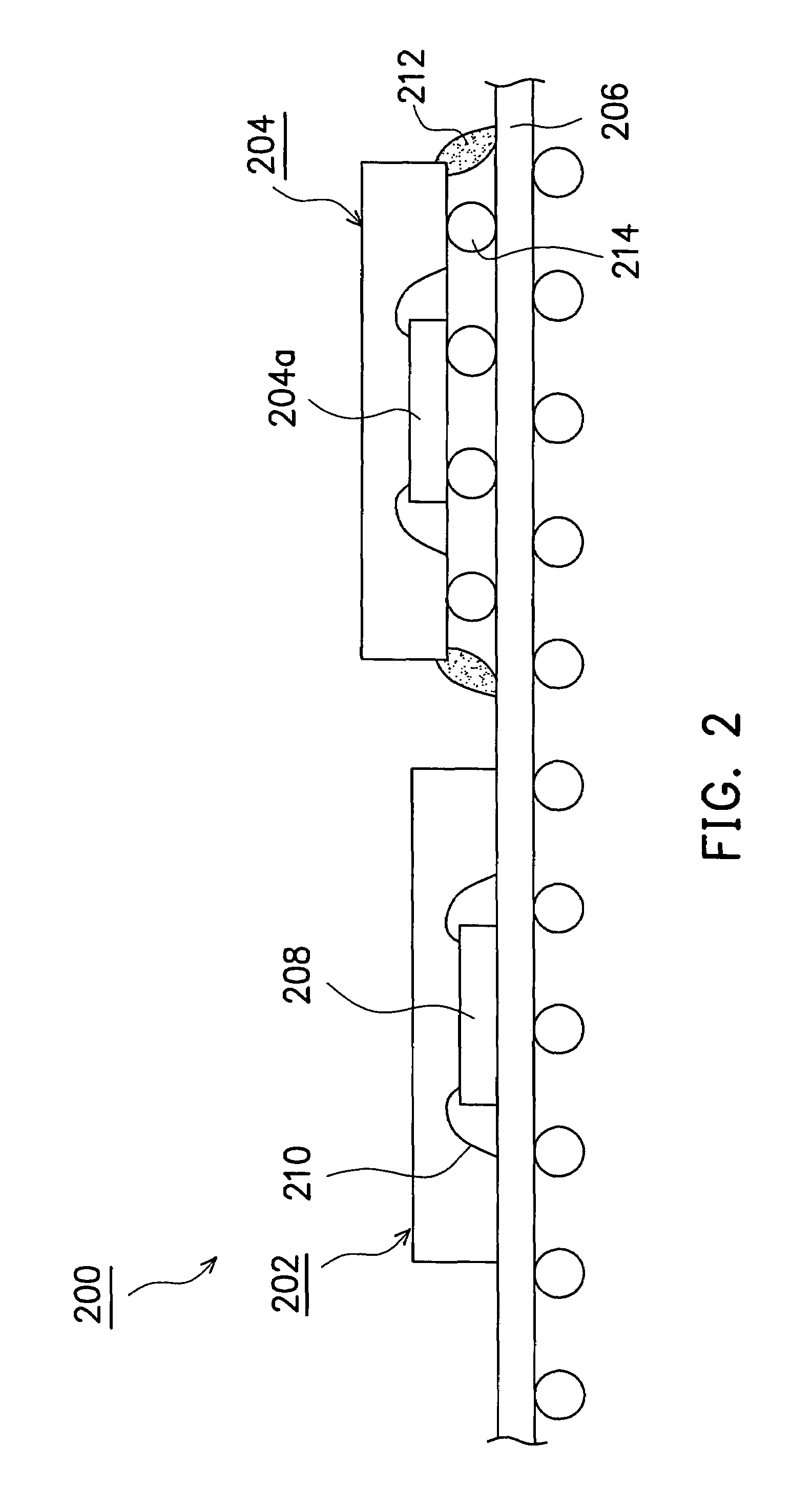
[0023]FIG. 2 is a schematic cross-sectional view of a semiconductor package according to one embodiment of the present invention. As shown in FIG. 2, the semiconductor package 200 mainly comprises a first semiconductor device 202 and a second semiconductor device 204. The first semiconductor device 202 and the second semiconductor device 204 are semiconductor packages. The first semiconductor device 202 comprises a substrate 206, a semiconductor chip 208 disposed on the substrate 206 and electrically connected to the semiconductor device 202 through a plurality of conductive wires 210. The second semiconductor device 204 is flip-chip bonded (for example, through a plurality of solder balls 214) to th...


PUM


Abstract

A semiconductor package comprising a substrate and a semiconductor device disposed on the substrate by flip-chip bonding. The present invention is characterized by a connection structure disposed between the semiconductor device and the substrate that extends along the periphery of the bottom surface of the semiconductor device. As a result, it can preferably provide additional mounting support between the two. The connection structure can be formed from cured adhesive. The present invention also provides a method of manufacturing the semiconductor package.

Description

BACKGROUND OF THE INVENTION[0001]1. Field of the Invention[0002]The present invention relates to a semiconductor package and method of manufacturing the same.[0003]2. Description of the Related Art[0004]FIG. 1 is a schematic cross-sectional view of a conventional semiconductor package. As shown in FIG. 1, the semiconductor package 100 has a semiconductor device 102 flip-chip bonded (for example, through a plurality of solder balls 108) to a substrate 104. An underfill layer 106 is formed in the space between the semiconductor device 102 and the substrate 104 to increase the mechanical strength of the bondage between the semiconductor device 102 and the substrate 104, and fix their positions relative to each other. Hence, the semiconductor package 100 is prevented from possible dissociation or deformation when it is subjected to a surface bonding process.[0005]However, moisture buried within the underfill layer 106 and volatile pollutants trapped on the surface of the semiconductor d...

Claims


Application Information

Patent Timeline
Patent Type & Authority Patents(United States)
IPC IPC(8): H01L23/48H01L23/40H01L23/52H01L23/02H05K3/30
CPCH05K3/305H05K2201/10734H05K2203/0545H01L2224/48091H01L2224/48227H01L2924/15311H01L2924/00014Y02P70/50
Inventor WENG, GWO-LIANGLU, YUNG-LICHU, CHI-CHIHLEE, SHIH-CHANG
Owner ADVANCED SEMICON ENG INC
Why Eureka
Try Eureka