Supercharge Your Innovation With Domain-Expert AI Agents!

Semiconductor memory device having an error correcting code circuit

a memory device and error correction technology, applied in error detection/correction, digital storage, instruments, etc., can solve problems such as soft errors, operating voltage, and static random access memory (sram) to pose problems

Inactive Publication Date: 2006-10-24
KK TOSHIBA
View PDF6 Cites 0 Cited by
  • Summary
  • Abstract
  • Description
  • Claims
  • Application Information

AI Technical Summary

Benefits of technology

This configuration reduces the worst-case fraction defective of multiple-bit errors and increases the overall error relief rate by balancing the defective rates across memory cells with different layout orientations, improving the reliability of error correction.

Problems solved by technology

With the advance in micropatterning technique and the decrease in operating voltage of semiconductor memory devices, soft errors in, e.g., static random access memories (SRAMs) have come to pose a problem.
However, an error of 2 or more bits cannot be corrected.
As the elements are micropatterned by scaling, and the voltage is decreased, the number of margin-based hard errors caused by the parasitic effect or element variation in the chip is increasing in addition to those which are caused by random reasons such as a crystal defect and dust.
The rate of such margin-based hard errors is not uniform and changes depending on the memory cell position.
As a result, the relief rate by ECC in the whole memory becomes low.

Method used


Image

  • Semiconductor memory device having an error correcting code circuit
  • Semiconductor memory device having an error correcting code circuit
  • Semiconductor memory device having an error correcting code circuit

Examples


first embodiment

(First Embodiment)

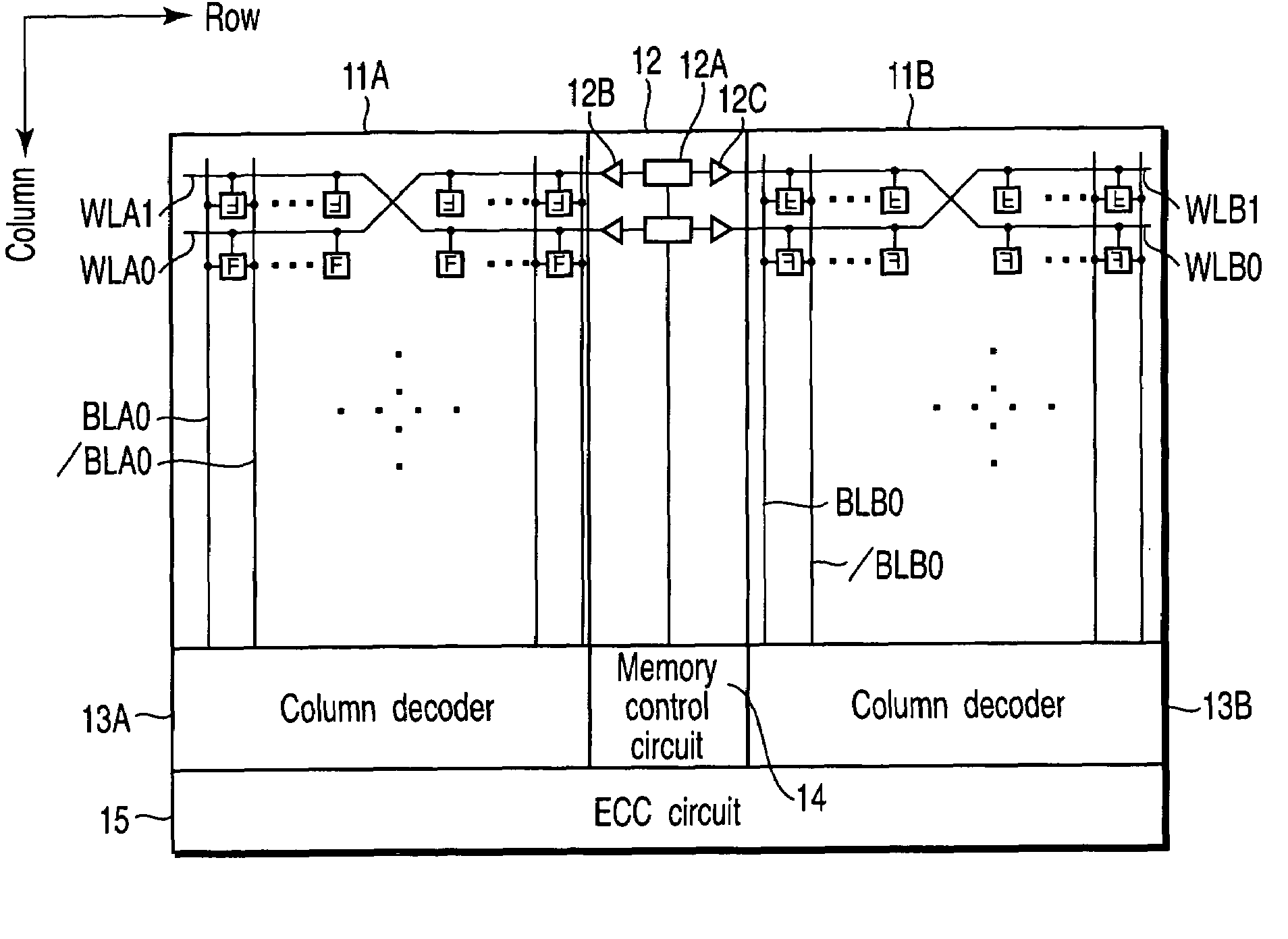
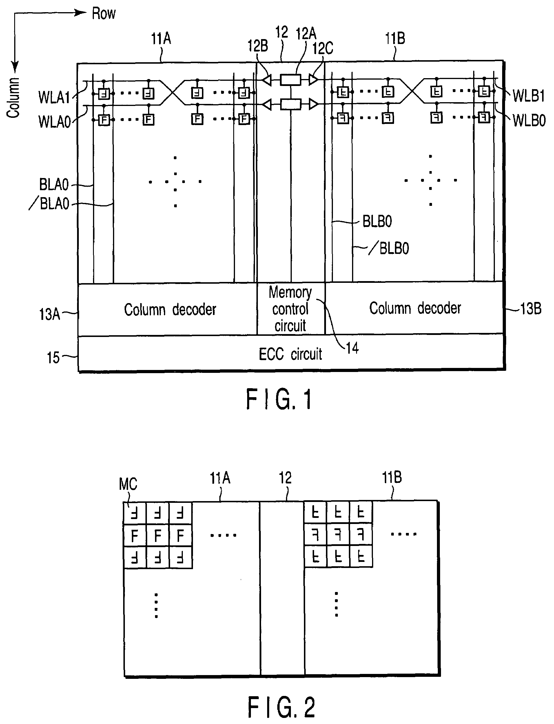
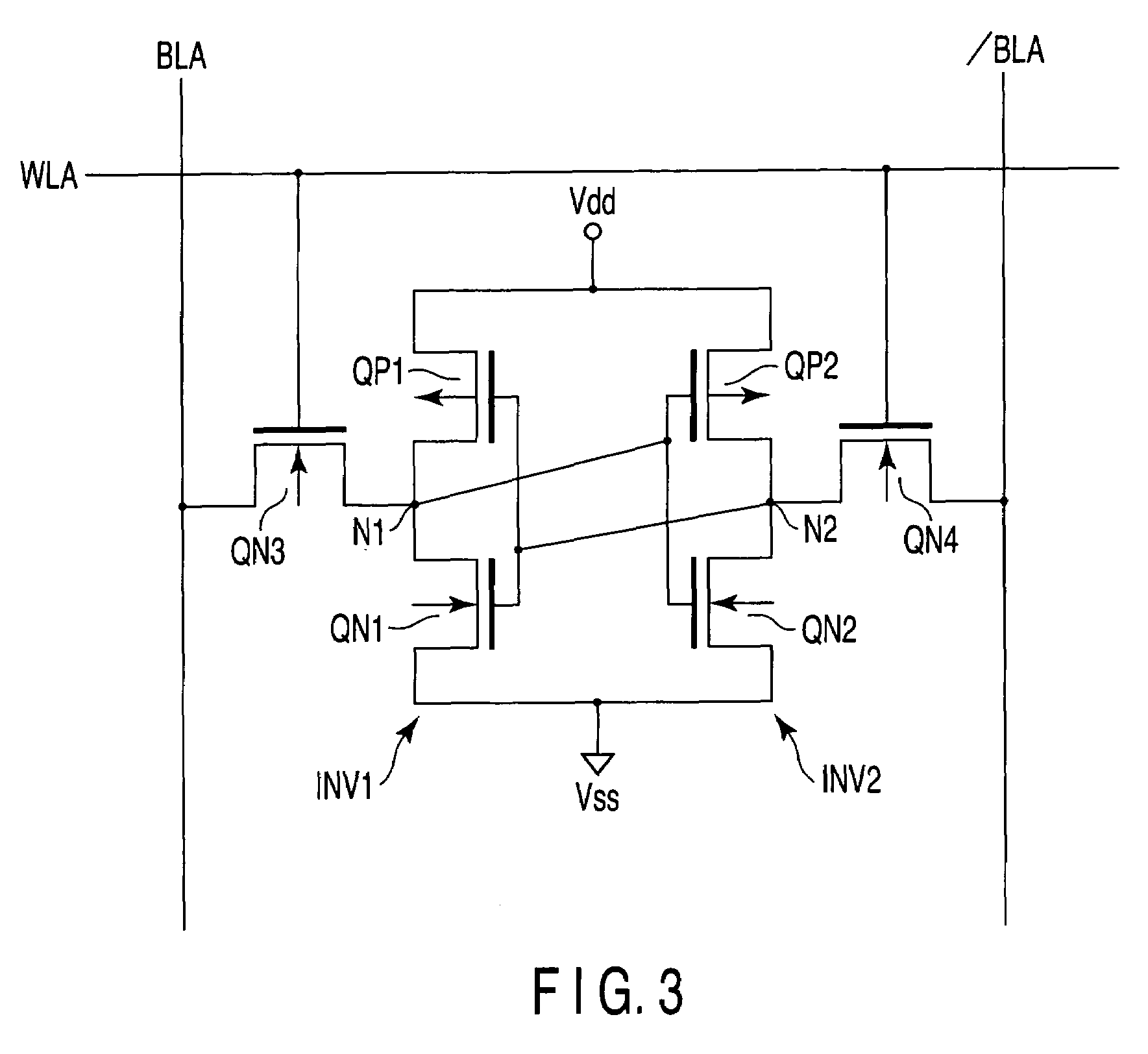
[0025]FIG. 1 is a block diagram showing the arrangement of a semiconductor memory device according to the first embodiment of the present invention. The semiconductor memory device comprises, e.g., two memory cell arrays 11A and 11B. A plurality of word lines WLA0 to WLAn running in the row direction are arranged in the memory cell array 11A. Additionally, a plurality of bit line pairs BLA0 to BLAm and / BLA0 to / BLAm running in the column direction are arranged in the memory cell array 11A.

[0026]A plurality of word lines WLB0 to WLBn running in the row direction are arranged in the memory cell array 11B. Additionally, a plurality of bit line pairs BLB0 to BLBm and / BLB0 to / BLBm running in the column direction are arranged in the memory cell array 11B.

[0027]A row decoder (row selection circuit) 12 is arranged between the memory cell array 11A and the memory cell array 11B. The row decoder 12 is connected to word lines WLA and WLB and selects the rows of the memory ...

second embodiment

(Second Embodiment)

[0067]In the second embodiment, the progress of the row address signal is changed between a memory cell array 21A and a memory cell array 21B.

[0068]FIG. 5 is a block diagram showing the arrangement of a semiconductor memory device according to the second embodiment of the present invention. Each of the memory cell arrays 21A and 21B includes a plurality of memory cells MC arranged in a matrix.

[0069]A row decoder 24 is arranged between the memory cell array 21A and the memory cell array 21B. The row decoder 24 is connected to word lines WLA and WLB and selects the rows of the memory cell arrays 21A and 21B.

[0070]The row decoder 24 comprises a plurality of output circuits 24C and 24D corresponding to the plurality of word lines. The output circuit 24C is connected to the word line WLA. The output circuit 24D is connected to the word line WLB.

[0071]A sense amplifier circuit (SA) 22A is arranged adjacent to a column decoder 13A. Data read out from the memory cell MC t...

third embodiment

(Third Embodiment)

[0092]In the third embodiment, the progress of the column address signal is changed between a memory cell array 21A and a memory cell array 21B.

[0093]FIG. 7 is a block diagram showing the arrangement of a semiconductor memory device according to the third embodiment of the present invention. Each of the memory cell arrays 21A and 21B includes a plurality of memory cells MC arranged in a matrix.

[0094]A row decoder 12 is arranged between the memory cell array 21A and the memory cell array 21B. The row decoder 12 is connected to word lines WLA and WLB and selects the rows of the memory cell arrays 21A and 21B.

[0095]A column decoder 31A is arranged at the column-direction end of the memory cell array 21A. The column decoder 31A is connected to a plurality of bit line pairs BLA0 to BLAm and / BLA0 to / BLAm. The column decoder 31A selects a column of the memory cell array 21A on the basis of a column address signal.

[0096]A column decoder 31B is arranged at the column-dire...


PUM


Abstract

A semiconductor memory device include includes a memory cell array which includes a first group of rows and a second group of rows, each row of the first group consisting of a plurality of first memory cells whose layout direction is a first direction, and each row of the second group consisting of a plurality of second memory cells whose layout direction is different from the first direction, a plurality of word lines which select rows of the memory cell array and each of which is connected to the first memory cells and second memory cells, and a plurality of bit line pairs which select columns of the memory cell array.

Description

CROSS-REFERENCE TO RELATED APPLICATIONS[0001]This application is based upon and claims the benefit of priority from prior Japanese Patent Application No. 2005-000788, filed Jan. 5, 2005, the entire contents of which are incorporated herein by reference.BACKGROUND OF THE INVENTION[0002]1. Field of the Invention[0003]The present invention relates to a semiconductor memory device and, more particularly, to a semiconductor memory device having an error correcting code (ECC) circuit.[0004]2. Description of the Related Art[0005]With the advance in micropatterning technique and the decrease in operating voltage of semiconductor memory devices, soft errors in, e.g., static random access memories (SRAMs) have come to pose a problem. The known soft errors are classified into those caused by α-rays emitted from a radioactive substance contained in the materials such as solder used for the semiconductor devices and those caused by fast neutrons arriving as cosmic rays.[0006]An effective measure...

Claims


Application Information

Patent Timeline
Patent Type & Authority Patents(United States)
IPC IPC(8): G11C16/06
CPCG06F11/1008G11C5/063G11C7/1006
Inventor HIRABAYASHI, OSAMU
Owner KK TOSHIBA
Features
  • R&D
  • Intellectual Property
  • Life Sciences
  • Materials
  • Tech Scout
  • Unparalleled Data Quality
  • Higher Quality Content
  • 60% Fewer Hallucinations
Learn More