Hybrid ground grid for printed circuit board

a printed circuit board and ground grid technology, applied in the direction of printed circuits, programmable/customizable/modifiable circuits, cross-talk/noise/interference reduction, etc., can solve the problems of reducing the available board space for such circuitry and components, imposing significant design limitations, and cumbersome design limitations

Inactive Publication Date: 2006-10-31
APPLE INC
View PDF3 Cites 85 Cited by
  • Summary
  • Abstract
  • Description
  • Claims
  • Application Information

AI Technical Summary

Benefits of technology

[0009]In accordance with the principles of the present invention, an improved electrical mounting board and methods for its fabrication and use are disclosed. In particular such improved boards utilize hybrid ground lines interconnected to form multilayer ground grids. Such implementations have many uses, including, but not limited to, the ability to more efficiently route signal lines and connect electrical components on a circuit board to ground line electrical paths.

Problems solved by technology

Such ground planes are satisfactory for certain purposes, but they impose certain significant design limitations.
On a two-layer board this can be a particularly cumbersome design limitation because it effectively prevents circuit structures and electronic components from being formed on or attached to the ground plane layer.
This cuts the available board space for such circuitry and components in half.
One significant drawback to the configuration depicted in FIG. 1 is that when all ground traces on a level are formed parallel to each other they impose significant restrictions on the configuration of any signal traces formed on the same level.
This is especially troublesome on two-level boards which cannot rely on the use of levels without ground grids to circumvent the restrictions imposed by the ground grids.
Additionally, signal traces cannot easily be formed extending in the “x”-axis direction because they would cross over other contacts 202.
However, in many cases, a designer cannot simply reorient the contacts to accommodate the ground grid.

Method used


Image

  • Hybrid ground grid for printed circuit board
  • Hybrid ground grid for printed circuit board
  • Hybrid ground grid for printed circuit board

Examples


Embodiment Construction

[0024]The present invention has been particularly shown and described with respect to certain embodiments and specific features thereof. The embodiments set forth hereinbelow are to be taken as illustrative rather than limiting. It should be readily apparent to those of ordinary skill in the art that various changes and modifications in form and detail may be made without departing from the spirit and scope of the invention.

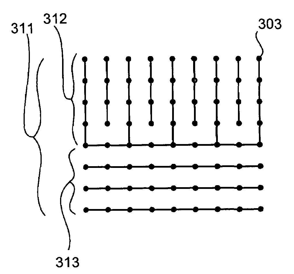
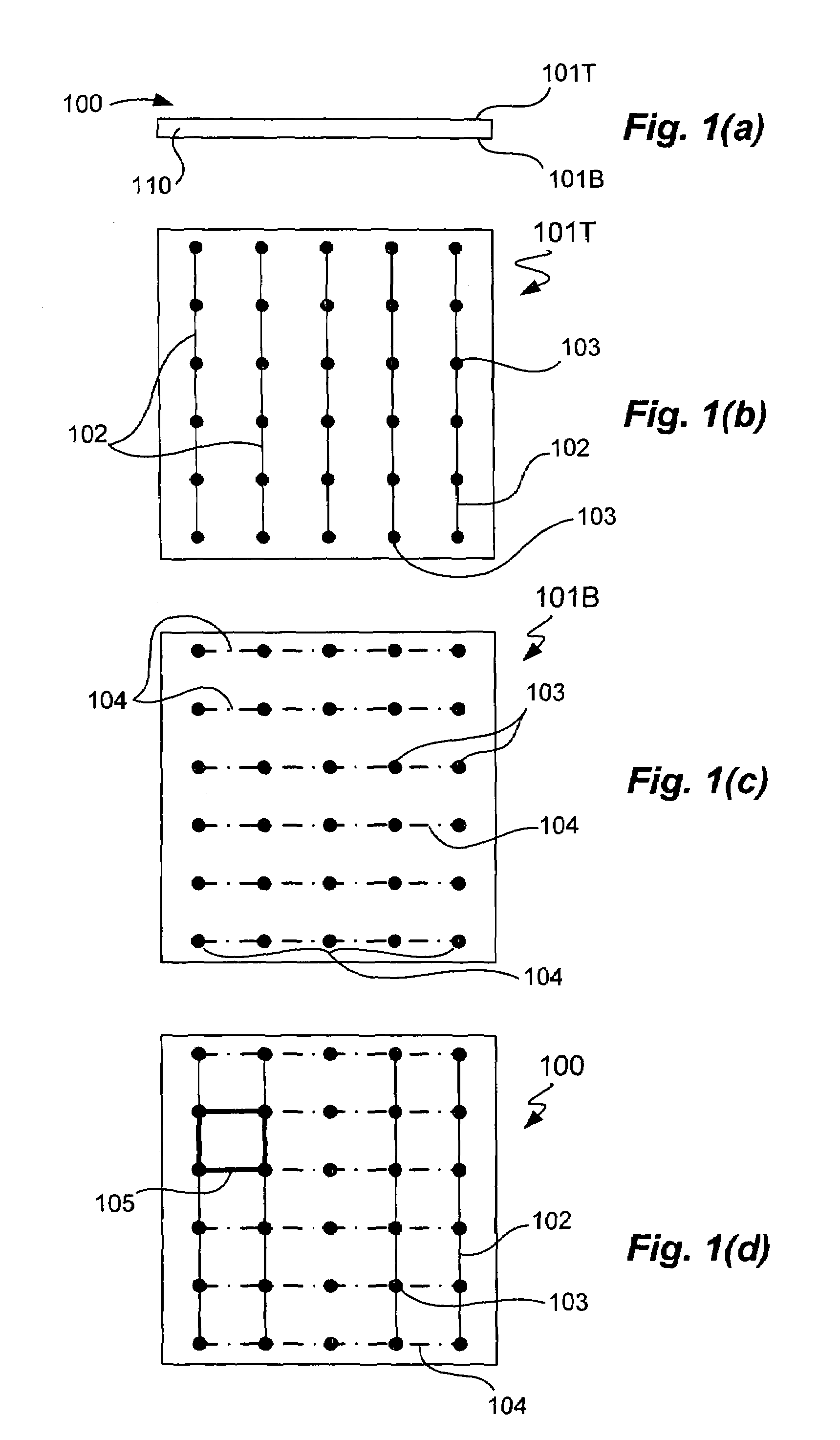
[0025]In the following detailed description, electrical circuit board embodiments will be disclosed. In particular, the depicted structures depict embodiments having hybrid ground layers integrated together to form suitable ground grid that can be electrically connected with circuits, components, and devices of the circuit board. Such embodiments provide improved circuit routing capability for signal traces as well as improved flexibility for the placement and orientation of electronic components used with the embodiments. Additionally, some embodiments can be co...


PUM

PropertyMeasurementUnit
electrically conductiveaaaaaaaaaa
electricalaaaaaaaaaa
areaaaaaaaaaaa

Abstract

Electrical mounting boards and methods for their fabrication and use are disclosed herein. In particular, such mounting boards embodiments utilize hybrid ground lines interconnected through a substrate core to form multilayer ground grids. Such hybrid ground lines include groups of substantially parallel ground lines configured such that the groups of ground lines are positioned in transverse arrangement with other groups of ground lines formed on the same level. Such implementations have many uses, including, but not limited to, the ability to more efficiently route signal lines and connect electrical components on a circuit board.

Description

TECHNICAL FIELD[0001]The invention described herein relates generally to printed wiring board layout. In particular, the invention relates to a printed circuit board construction having a hybrid grid network of ground traces formed on two or more layers of the printed circuit board to provide electrical paths capable of reducing Electromagnetic Emissions and improving the Electromagnetic Immunity performance as well as being capable of accommodating a wide range of component arrangements and signal trace configurations.BACKGROUND[0002]In conventional circuit mounting boards (e.g., printed circuit boards (PCB's)) a ground plane is formed on one or more layers of the board. Such ground planes can be formed on the top or bottom surfaces of boards (especially using basic two layer boards). Also, such ground planes can be formed on interior layers of multi-layer (three or more layers) boards. Such ground planes are satisfactory for certain purposes, but they impose certain significant de...

Claims


Application Information

Patent Timeline
Patent Type & Authority Patents(United States)
IPC IPC(8): H05K1/03
CPCH05K1/0219H05K1/0289Y10T29/49117H05K2201/09236H05K2201/09972H05K1/0298
Inventor STEINFELD, ROBERTLAM, CHEUNG-WEI
Owner APPLE INC
Why Eureka
Try Eureka