Methods and systems for inspection of an entire wafer surface using multiple detection channels

a technology of wafer surface and detection channel, applied in the direction of optically investigating flaws/contamination, instruments, measurement devices, etc., can solve the problems of untraceable yield loss, catastrophic wafer breakage, cross contamination during processing,

Active Publication Date: 2006-10-31
KLA TENCOR TECH CORP
View PDF29 Cites 32 Cited by
  • Summary
  • Abstract
  • Description
  • Claims
  • Application Information

AI Technical Summary

Benefits of technology

[0011]In another embodiment, the method may include collecting the light scattered from the center and edge portions of the wafer with a single collection channel. Such a method may also include directing the light collected by the single collection channel to the first and second detection channels. In some embodiments, the method may include collecting the light scatter

Problems solved by technology

The main concerns are that edge defects could fall onto the central part of the wafer thereby causing untraceable yield loss, cross contamination during processing, and/or catastrophic wafer breakage.
These yield loss mechanisms are experienced by most wafer and IC manufacturers at one time or another.
As a result, these large amounts of light will saturate the detectors of traditional wafer inspection systems.
Consequently, any output signals generated near or at the edge of wafers by such wafer inspection tools are generally unusable.
Therefore, the edge inspection systems are not optimized to, or even able to, detect defects in the central portion of the wafers.
Consequently, if wafer or IC manufacturers want to detect defects in both the central and o

Method used


Image

  • Methods and systems for inspection of an entire wafer surface using multiple detection channels
  • Methods and systems for inspection of an entire wafer surface using multiple detection channels
  • Methods and systems for inspection of an entire wafer surface using multiple detection channels

Examples


Embodiment Construction

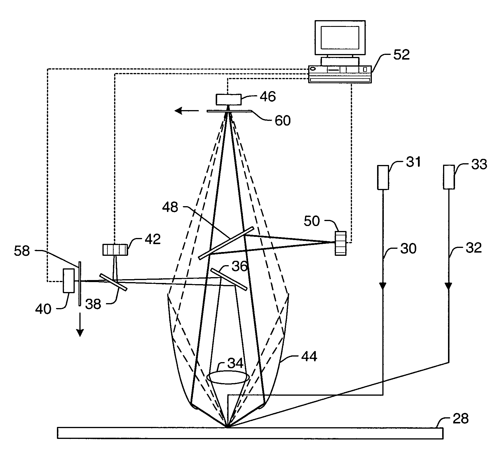
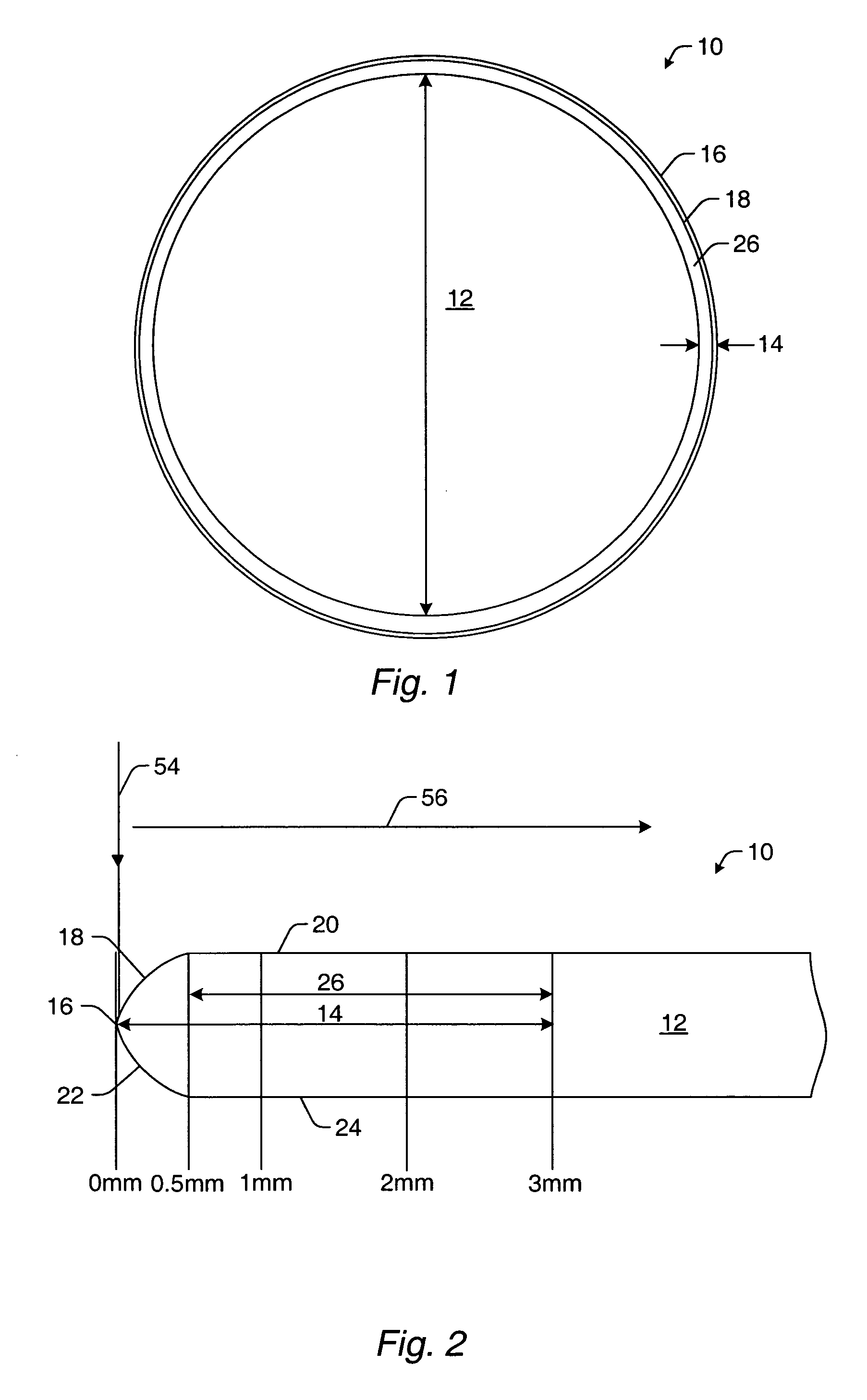
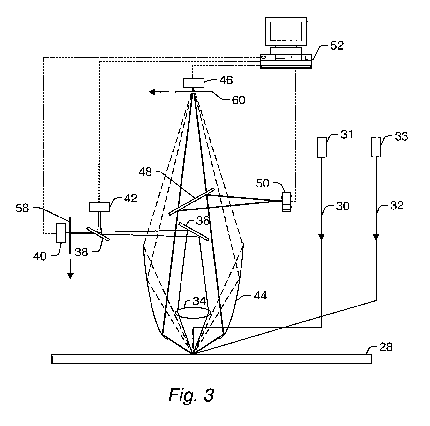
[0021]As used herein, the term “wafer” generally refers to substrates formed of a semiconductor or non-semiconductor material. Examples of such a semiconductor or non-semiconductor material include, but are not limited to, monocrystalline silicon, gallium arsenide, and indium phosphide. Such substrates may be commonly found and / or processed in semiconductor fabrication facilities.

[0022]A wafer may include only the substrate such as a virgin wafer. Alternatively, a wafer may include one or more layers that may be formed upon a substrate. For example, such layers may include, but are not limited to, a resist, a dielectric material, and a conductive material. A resist may include a resist that may be patterned by an optical lithography technique, an e-beam lithography technique, or an X-ray lithography technique. Examples of a dielectric material may include, but are not limited to, silicon dioxide, silicon nitride, silicon oxynitride, and titanium nitride. Additional examples of a die...


PUM


Abstract

Methods for inspecting a wafer are provided. One method includes directing light to a center portion and an edge portion of a wafer in a single scan. The method also includes detecting light scattered from the center portion using a first detection channel and detecting light scattered from the edge portion using a second detection channel. Another method for inspecting an edge portion of a wafer includes scanning the edge portion of the wafer with light. The method also includes separately detecting different portions of light scattered from the edge portion. In addition, the method includes separating light scattered from edge features in the edge portion from other light scattered from the edge portion. The method further includes detecting defects in the edge portion of the wafer using the other scattered light.

Description

BACKGROUND OF THE INVENTION[0001]1. Field of the Invention[0002]The present invention generally relates to methods and systems for inspection of an entire wafer surface using multiple channels. Certain embodiments relate to detecting light scattered from different portions of the entire wafer surface using different detection channels.[0003]2. Description of the Related Art[0004]Fabricating semiconductor devices such as logic and memory devices typically includes processing a specimen such as a semiconductor wafer using a number of semiconductor fabrication processes to form various features and multiple levels of the semiconductor devices. For example, lithography is a semiconductor fabrication process that typically involves transferring a pattern to a resist arranged on a semiconductor wafer. Additional examples of semiconductor fabrication processes include, but are not limited to, chemical-mechanical polishing, etch, deposition, and ion implantation. Multiple semiconductor devi...

Claims


Application Information

Patent Timeline
IPC IPC(8): G01N21/88
CPCG01N21/47G01N21/9501G01N21/9503G01N21/95607G01N21/95623
Inventor KUHLMANN, LIONELMCMILLAN, WAYNE
Owner KLA TENCOR TECH CORP
Why Eureka
Try Eureka