
Integrated semiconductor device providing for preventing the action of parasitic transistors

a semiconductor device and parasitic transistor technology, applied in the field of semiconductor devices, can solve the problems of inordinate space requirements, substantial addition of semiconductor devices, and unavoidable creation of parasitic transistors between neighboring ones of the transistors of each motor driver circuit, and achieve the effect of preventing the undesired action

Active Publication Date: 2006-11-14
SANKEN ELECTRIC CO LTD
View PDF1 Cites 1 Cited by
  • Summary
  • Abstract
  • Description
  • Claims
  • Application Information

AI Technical Summary

Benefits of technology

This solution effectively prevents parasitic transistor conduction, ensuring accurate motor control and reducing current loss, while significantly reducing the size of the semiconductor device compared to prior art methods.

Problems solved by technology

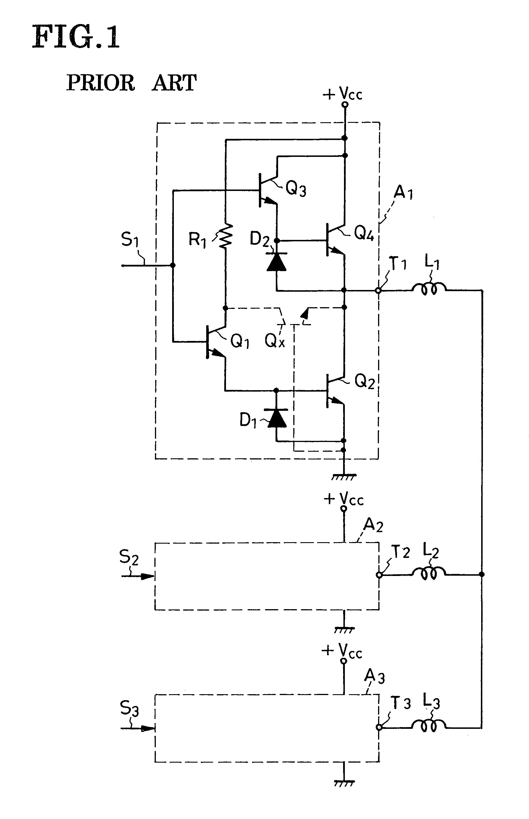
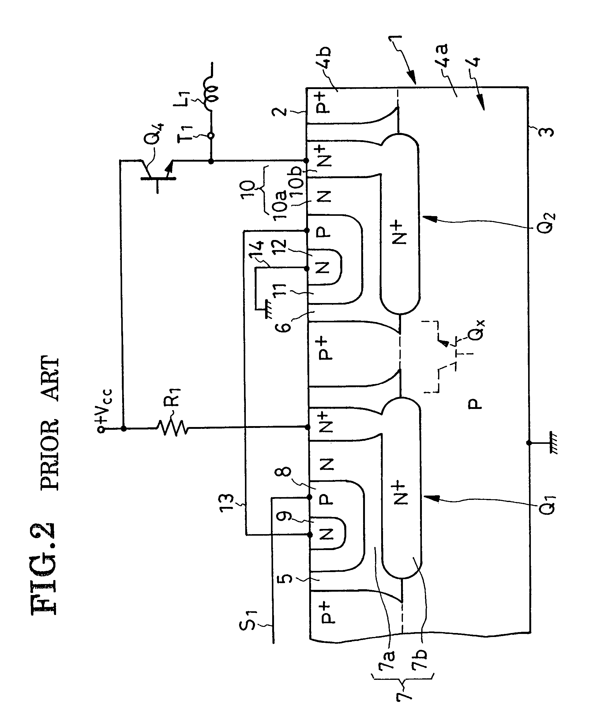
When the motor driver circuits were fabricated in the form of an integrated semiconductor circuit (FIG. 2), a parasitic transistor was unavoidably created between two neighboring ones of the transistors of each motor driver circuit.
An objection to this prior art device is its inordinate space requirement between the transistors, adding substantively to the size of the semiconductor device.

Method used


Image

  • Integrated semiconductor device providing for preventing the action of parasitic transistors
  • Integrated semiconductor device providing for preventing the action of parasitic transistors
  • Integrated semiconductor device providing for preventing the action of parasitic transistors

Examples


first embodiment

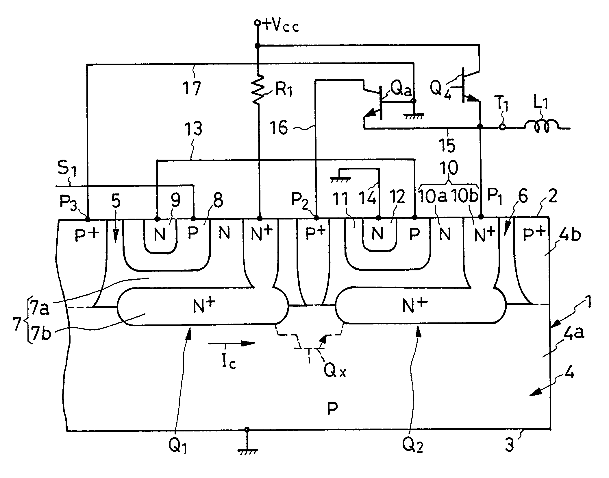
[0051]The advantages gained by this first embodiment of the invention may be summarized as follows:

[0052]1. The performance-enhancer transistor Qa positively prevents the parasitic transistor Qx from becoming active when the driver output T1 goes negative in potential, so that the motor drive system is protected from erroneous operation, resulting in more accurate control of motor operation.

[0053]2. Current loss due to the performance-enhancer transistor Qa is reducible by making the substrate region 4a appropriately high in resistance.

[0054]3. The integrated semiconductor device is appreciably reduced in size compared to the prior art devices that attain the same objective by spacing the transistors Q1 and Q2 far enough away from each other or by providing a floating region therebetween.

embodiment

of FIG. 6

[0055]FIG. 6 shows another preferred form of integrated semiconductor device according to the invention, in a sectional view similar to FIG. 5. This alternative embodiment does not have the performance-enhancer transistor Qa of the FIGS. 3–5 embodiment but does incorporate, instead, a third n-type island-like semiconductor region 30 in the semiconductor substrate 1. This third island-like region 30 is designed for intentional creation of an additional parasitic transistor Qb in coaction with the preexisting second transistor Q2 in order to preclude the harmful effect of the undesired parasitic transistor Qx. The additional parasitic transistor Qb will therefore be hereinafter referred to as the performance-enhancer parasitic transistor.

[0056]Referring more specifically to FIG. 6, the third island-like region 30 is arranged on that side of the second transistor Q2 which is opposite to the side where there lies the first transistor Q1. The undesired parasitic transistor Qx ex...


PUM


Abstract

An electric motor drive system is disclosed which includes a required number of motor driver circuits connected one to each motor armature coil. Fabricated in the form of an integrated circuit, each such motor driver circuit has a parasitic transistor unavoidably created between two neighboring transistors. The parasitic transistor would become conductive when the driver circuit output had a negative potential, adversely affecting the driver circuit operation. An additional transistor is provided in one embodiment of the invention in order to inhibit such action of the parasitic transistor. Becoming conductive when the driver circuit output goes negative, the additional transistor prevents conduction through the parasitic transistor. Another parasitic transistor is intentionally created in another embodiment for the same purpose.

Description

CROSS REFERENCE TO RELATED APPLICATIONS[0001]This application claims priority to Japanese Application No. 2003-334680, filed Sep. 26, 2003.BACKGROUND OF THE INVENTION[0002]This invention relates to semiconductor devices in general and, in particular, to those especially well adapted for use in the electronic driver circuits of electric motors, among other applications. More particularly, the invention pertains to an integrated semiconductor device incorporating transistors or like active elements, featuring provisions for inhibiting or restricting the action of parasitic transistors under certain foreseeable conditions in use of the semiconductor device in motor drive systems or the like.[0003]Japanese Unexamined Patent Publication No. 63-18660 is hereby cited as teaching a motor drive system (FIG. 1) representing a typical application of the instant invention. The motor drive system has a required number of motor driver circuits of like construction coupled one to each of the motor...

Claims


Application Information

Patent Timeline
Patent Type & Authority Patents(United States)
IPC IPC(8): H01L29/00H01L21/331H01L21/761H01L21/8222H01L27/06H01L27/082H01L29/732
CPCH01L21/761H01L27/0823
Inventor UEHARA, DAIJINAKAMURA, HIROAKI
Owner SANKEN ELECTRIC CO LTD
Learn More