Circuit substrate device, method for producing the same, semiconductor device and method for producing the same

a substrate device and circuit substrate technology, applied in the direction of printed circuit manufacturing, printed circuit aspects, basic electric elements, etc., can solve the problems of reducing production efficiency, affecting the production efficiency of semiconductor chips, so as to improve production efficiency, reduce production time appreciably, and fine line width

Inactive Publication Date: 2006-11-21
SONY CORP
View PDF5 Cites 3 Cited by
  • Summary
  • Abstract
  • Description
  • Claims
  • Application Information

AI Technical Summary

Benefits of technology

[0038]With the present method for producing a semiconductor device, it is checked in the inspection step, whether or not the pattern conductor has been formed properly, from one circuit unit of the circuit set to another, and the multi-layer wiring substrate is bonded in the bonding step only to the circuit unit of the circuit set where the pattern conductor has been formed properly. After the dummy substrate has been removed in the removing step, the resulting circuit substrate set is split in the splitting step, on the circuit unit basis, with the circuit set remaining attached to the multi-layer wiring substrate, whereby a plural number of the circuit substrates, each composed of the multi-layer wiring substrate bonded to the satisfactory circuit unit, may be produced in a lump, thus improving the production efficiency and decreasing the production time appreciably.
[0039]Additionally, with the present method for producing a semiconductor device, in which the dummy substrate is removed after bonding the multi-layer wiring substrate to the circuit set, such a semiconductor device may be produced including a circuit substrate unit having a circuit unit on the major surface of the multi-layer wiring substrate, with the pattern conductor being free from warping or inundations along the thickness and being formed to fine line width and to high accuracy. With the present invention, a circuit unit is formed via a release layer on a dummy substrate, having a flattened out surface, with the dummy substrate and the release layer being removed after bonding the circuit unit having the pattern conductor by the thin film technique is bonded to the multi-layer wiring substrate. As a result, the circuit substrate device and the semiconductor device, suppressed in warping and inundations along the thickness of the circuit unit, may be produced.
[0040]Thus, according to the present invention, the circuit unit, including a pattern conductor, as a fine line formed to a high density and a high accuracy, may be formed on the multi-layer wiring substrate, so that a circuit substrate device, improved in electrical characteristics and reduced in size, and a semiconductor device, having a semiconductor chip mounted on this circuit substrate device, may be produced.
[0041]Moreover, according to the present invention, the circuit unit, found to be defective as to the pattern conductor in the inspection step, may be prohibited from being bonded to the multi-layer wiring substrate, so that it is possible to improve the production efficiency and to lower the cost in producing the circuit substrate device or the semiconductor device. Additionally, since plural circuit substrate devices can be formed in a lump by employing the circuit set or the substrate set, it is also possible to decrease the production time and to improve the production efficiency in producing the circuit substrate device or the semiconductor device. Since the dummy substrate can be re-used, it is possible to decrease the cost further cost in producing the circuit substrate device or the semiconductor device.

Problems solved by technology

Moreover, in producing the multi-layer wiring substrate 100, the manufacturing process may be complex with the increasing number of the layers of the pattern conductors 101 to increase the production time or to lower the production efficiency.
However, with the Si substrate or the glass substrate, it is difficult to form e.g., via-holes, such that electrode lands, operating as connection terminals for a motherboard, cannot be formed on a surface on the opposite side of the mounting surface for the semiconductor chip, with the consequence that these substrates cannot be used as mounting substrates for the semiconductor chips.

Method used


Image

  • Circuit substrate device, method for producing the same, semiconductor device and method for producing the same
  • Circuit substrate device, method for producing the same, semiconductor device and method for producing the same
  • Circuit substrate device, method for producing the same, semiconductor device and method for producing the same

Examples


Embodiment Construction

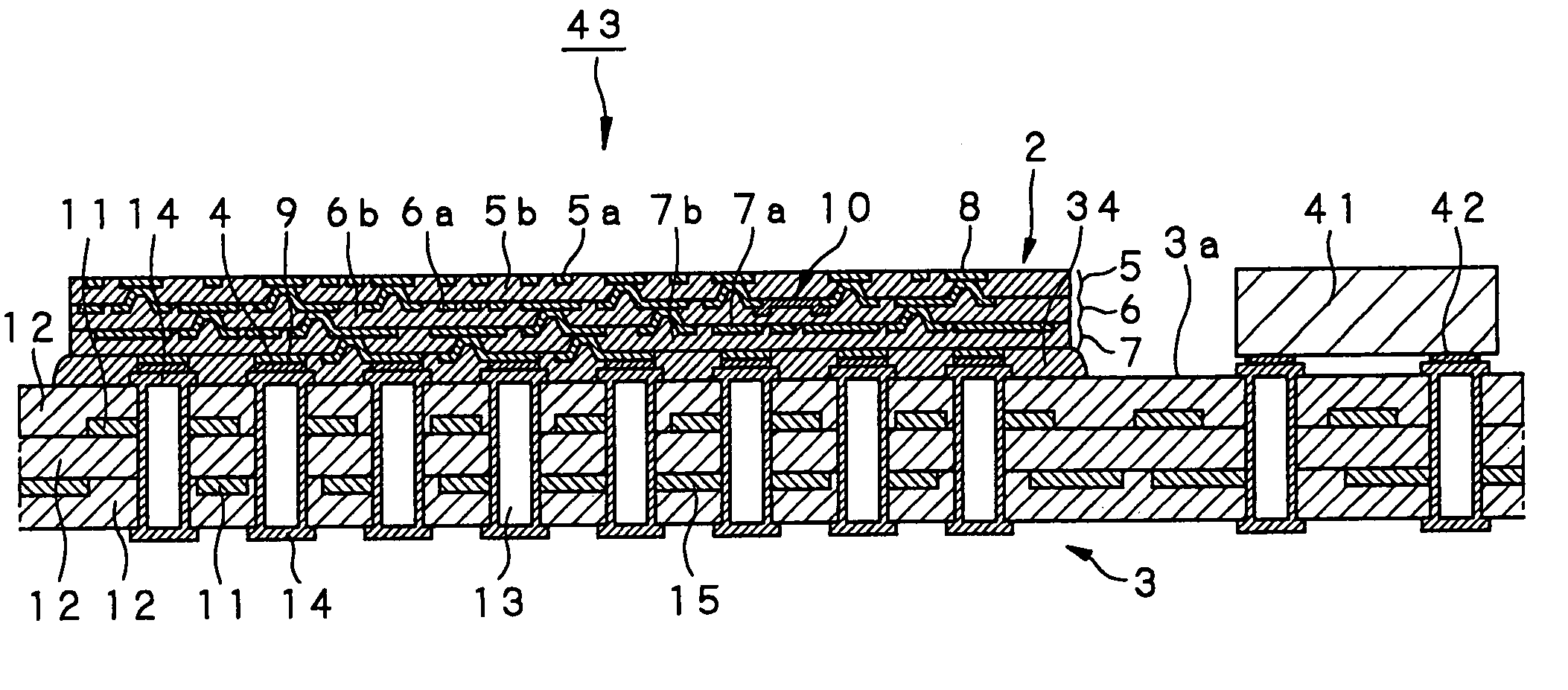
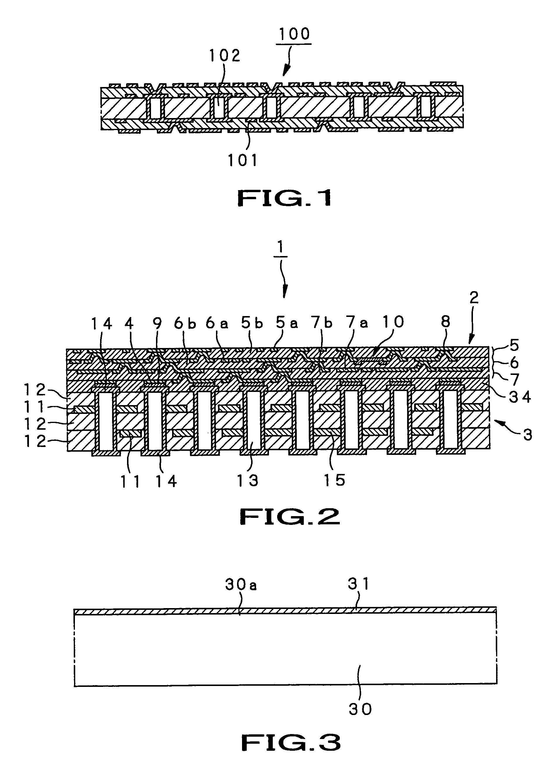
[0056]Referring to the drawings, a first embodiment of the present invention will be explained in detail. A circuit substrate device 1, shown as an embodiment in FIG. 2, includes a circuit unit 2, electrically connected to a multi-layer wiring substrate 3 by for example a bump unit 4, such as solder. The circuit unit 2 operates as a high frequency circuit performing e.g., a switching operation for high frequency signals, in a superheterodyne system or a direct conversion system, in a transmitting / receiving unit provided in e.g., a portable, communication terminal equipment.

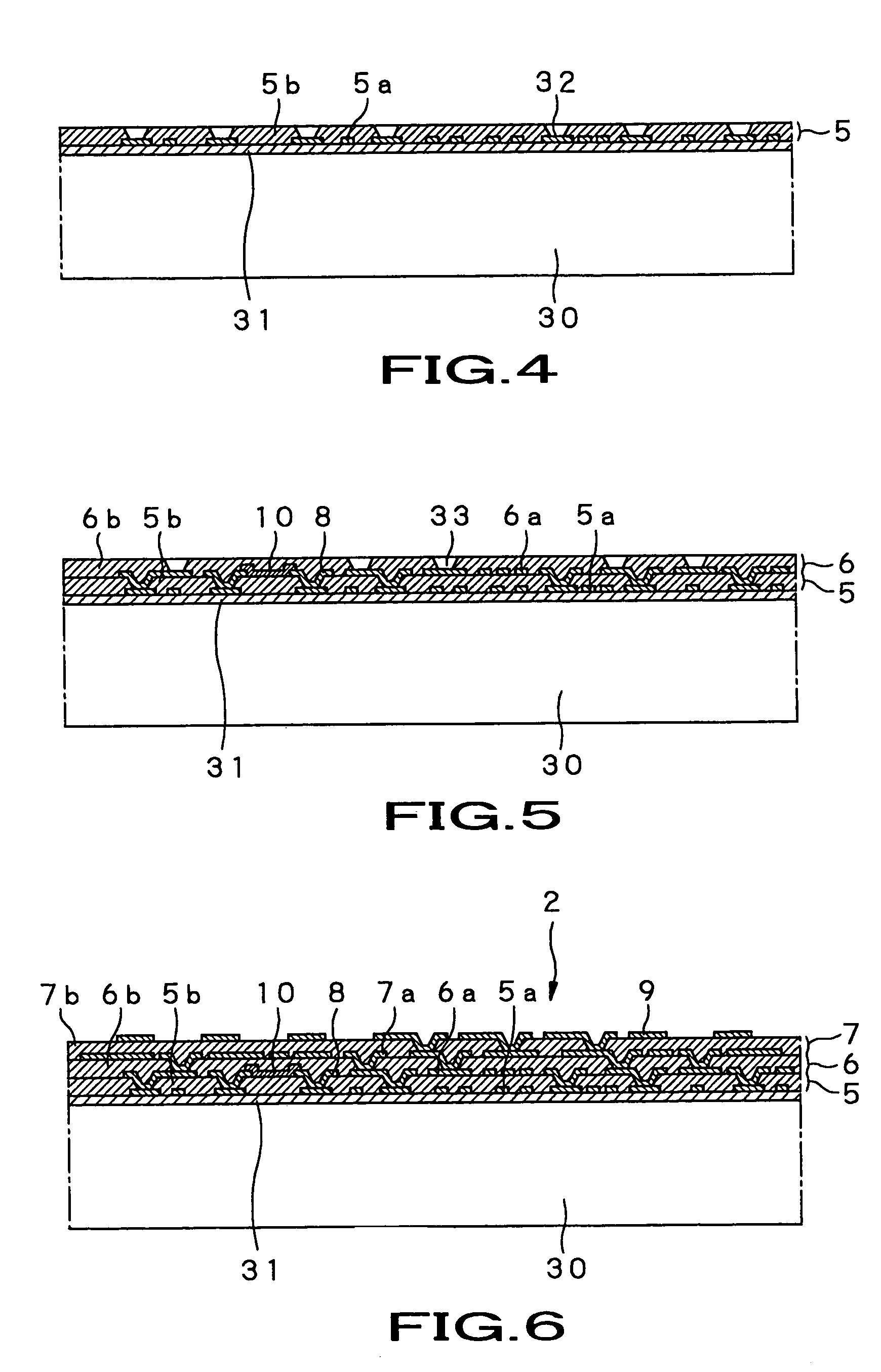
[0057]The circuit unit 2 is made up by a first unit wiring layer 5, a second unit wiring layer 6 formed on the major surface of the first unit wiring layer and a third unit wiring layer 7 formed on the major surface of the a second unit wiring layer 6. Each of the layers 5 to 7 is composed of an insulating layer and a pattern conductor.

[0058]The layers 5 to 7 of the circuit unit 2 are electrically interconnected b...


PUM


Abstract

A circuit substrate device composed of a circuit unit 2 and a multi-layer wiring substrate 3 in which a pattern conductor of the circuit unit 2 may be prevented from being warped or inundated. The circuit substrate device includes a circuit unit 2 having a pattern conductor formed by a thin film technique, and an insulating layer, and a multi-layer wiring substrate 3 having a connecting terminal portion 14 exposed from its major surface. The circuit unit is formed on a dummy substrate. The circuit unit is connected to the multi-layer wiring substrate 3 so that the pattern conductor is connected to the connecting terminal portion 14. The dummy substrate is then removed to give a structure comprised of the circuit unit 2 formed on the multi-layer wiring substrate 3. The pattern conductor of the circuit unit 2 is freed of warping or inundations along the direction of thickness of the circuit unit 2.

Description

[0001]The subject matter of application Ser. No. 10 / 397,608 is incorporated herein by reference. The present application is a divisional of U.S. application Ser. No. 10 / 397,608, filed Mar. 26, 2003 now U.S. Pat. No. 6,831 357, which claims priority to Japanese Patent Application No. JP2002-105549, filed Apr. 8, 2002. The present application claims priority to these previously filed applications.BACKGROUND OF THE INVENTION[0002]1. Field of the Invention[0003]This invention relates to a circuit substrate device, on which a pattern conductor has been formed properly, a method for producing the same, a semiconductor device, and a method for producing the same. This application claims priority of Japanese Patent Application No. 2002-105549, filed on, 2002, the entirety of which is incorporated by reference herein.[0004]2. Description of Related Art[0005]Recently, there is raised a demand for a technique of mounting functional elements, such as semiconductor chips, on e.g., a substrate, t...

Claims


Application Information

Patent Timeline
Patent Type & Authority Patents(United States)
IPC IPC(8): H01L21/44H05K3/00H01L21/48H01L21/68H01L23/12H01L23/498H05K3/20H05K3/46
CPCH01L21/4857H01L21/6835H01L23/49833H05K3/4602H05K3/4682H05K3/4694H01L2221/68345H01L2221/68359H01L2224/16H01L2924/01078H01L2924/09701H01L2924/19041H05K3/0052H05K3/20H05K3/4614H05K3/467H05K2201/0352H05K2201/09536H05K2203/061H01L2924/01087
Inventor NISHITANI, YUJIOGAWA, TSUYOSHIASAMI, HIROSHIOKUBORA, AKIHIKO
Owner SONY CORP
Why Eureka
Try Eureka