

High-frequency device
a high-frequency device and high-frequency technology, applied in the direction of duplex signal operation, resonant antenna, instruments, etc., can solve the problems of large size of high-frequency devices and insufficient characteristics of conventional high-frequency devices
- Summary
- Abstract
- Description
- Claims
- Application Information
AI Technical Summary
Benefits of technology
Problems solved by technology
Method used
Image

Examples
embodiment 1
(Embodiment 1)
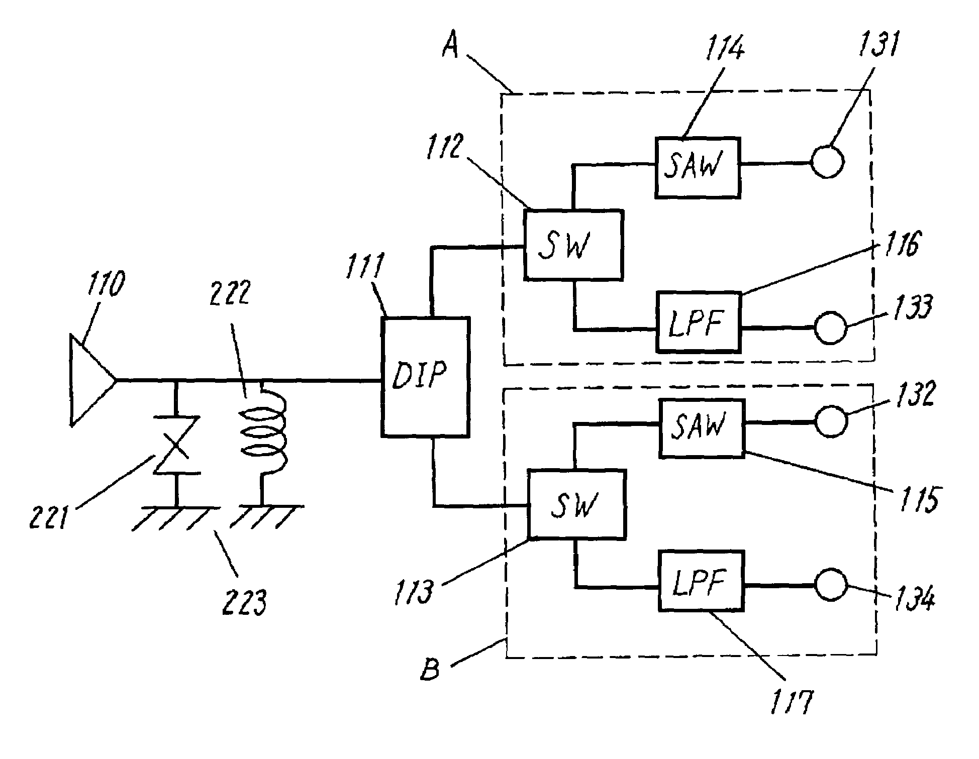
[0040]FIG. 1 is a circuit block diagram of a high-frequency device according to exemplary embodiment 1. The high-frequency device can be used as an antenna duplexer in a mobile telephone of the GSM / DCS dual band communications system, which is standardized in Europe. An antenna terminal 110 is connected to a diplexer 111 for separating and combining respective signals of the GSM band and the DCS band. In FIG. 1, a portion A processes the signal of the GSM band, and a portion B processes the signal of the DCS band. The diplexer 111 is connected to switches 112 and 113 for switching between a transmission and a reception. The switches 112 and 113 are connected to low pass filters (LPFs) 116 and 117 and connected to SAW filters 114 and 115 functioning as band pass filters for passing desired frequency bands, respectively. The filters 114, 115, 116, and 117 are connected to ports 131, 132, 133, and 134, respectively. The switches 112 and 113 are implemented by semiconducto...
embodiment 2
(Embodiment 2)
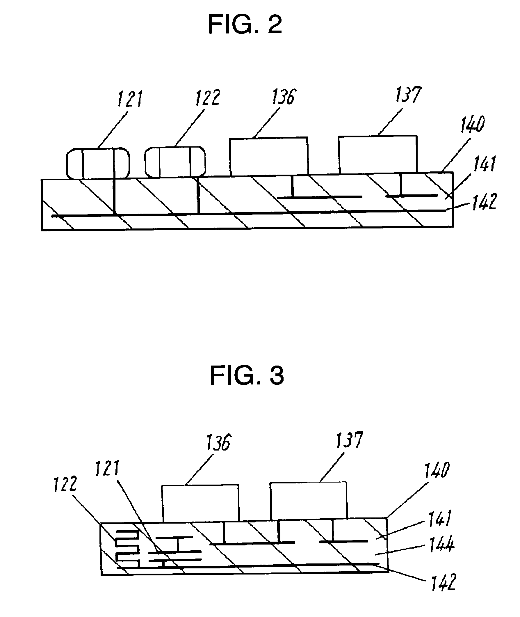
[0052]FIG. 2 is a cross sectional view of a high-frequency device according to exemplary embodiment 2 of the present invention. A circuit of the high-frequency device is identical to that of embodiment 1 shown in FIG. 1 and will be explained in no more detail.
[0053]As shown in FIG. 2, a ceramic laminated substrate 140 includes ceramic layers 141 and conductive patterns 142 stacked alternately. An antenna terminal 110, a diplexer 111, switches 112 and 113 excluding diodes, LPFs 116 and 117, and ports 131, 132, 133, and 134 (not shown) are provided on and in the ceramic laminated substrate 140. A diode 136, a SAW filter 137, a capacitor 121, and an inductor 122 are surface-mounted on the upper side of the ceramic laminated substrate 140, thus forming the circuit identical to that shown in FIG. 1. The SAW filter 137 includes SAW filters 114 and 115 assembled in a package.
[0054]Since including such components integrated, the high-frequency device of embodiment 2 can have a...
embodiment 3
(Embodiment 3)
[0056]FIG. 3 is a cross sectional view of a high-frequency device according to exemplary embodiment 3 of the present invention. A circuit of the high-frequency device is identical to that of embodiment 1 shown in FIG. 1 and will be explained in no more detail.
[0057]The high-frequency device of embodiment 3 includes a capacitor 121 and an inductor 122 having shapes different from those of embodiment 2.
[0058]According to embodiment 3, as shown in FIG. 3, an antenna terminal 110, a diplexer 111, switches 112 and 113 excluding diodes, LPFs 116 and 117, and ports 131, 132, 133, and 134 (not shown) are provided on and in a ceramic laminated substrate 140 including ceramic layers 141 and conductive patterns 142 stacked alternately. During the fabrication of the ceramic laminated substrate 140, the capacitor 121 is formed by forming a ceramic layer 144 made of ceramic material together with internal electrodes 145 in the substrate 140 simultaneously to forming of the inductor ...
PUM
 Abstract
Description
Claims
Application Information