Semiconductor memory devices having extending contact pads and related methods

a technology of contact pads and memory devices, which is applied in the direction of semiconductor devices, semiconductor/solid-state device details, electrical apparatus, etc., can solve the problems of many boundaries and a long contact path length, high contact resistance in a complete semiconductor memory device, and high contact resistance, so as to reduce contact path length and contact resistance, and improve electrical contact conductivity and productivity.

Active Publication Date: 2006-12-05
SAMSUNG ELECTRONICS CO LTD
View PDF17 Cites 4 Cited by
  • Summary
  • Abstract
  • Description
  • Claims
  • Application Information

AI Technical Summary

Benefits of technology

[0010]Accordingly, embodiments of the invention may provide reduced contact path length and contact resistance in capacitor contacts and bit line contacts. Electrical contact conductivity and productivity may be improved.

Problems solved by technology

According to the above-described conventional methods, the lower electrode contact and the bit line contact are typically formed through different processes, resulting in many boundaries and a long contact path length.
As a result, the contact resistance in a complete semiconductor memory device may be substantially high and short-circuiting may be likely to occur due to the introduction of dopants in the complicated manufacturing process.
Therefore, the conventional techniques may lower the yield and reliability of semiconductor memory devices produced thereby.

Method used


Image

  • Semiconductor memory devices having extending contact pads and related methods
  • Semiconductor memory devices having extending contact pads and related methods
  • Semiconductor memory devices having extending contact pads and related methods

Examples


Embodiment Construction

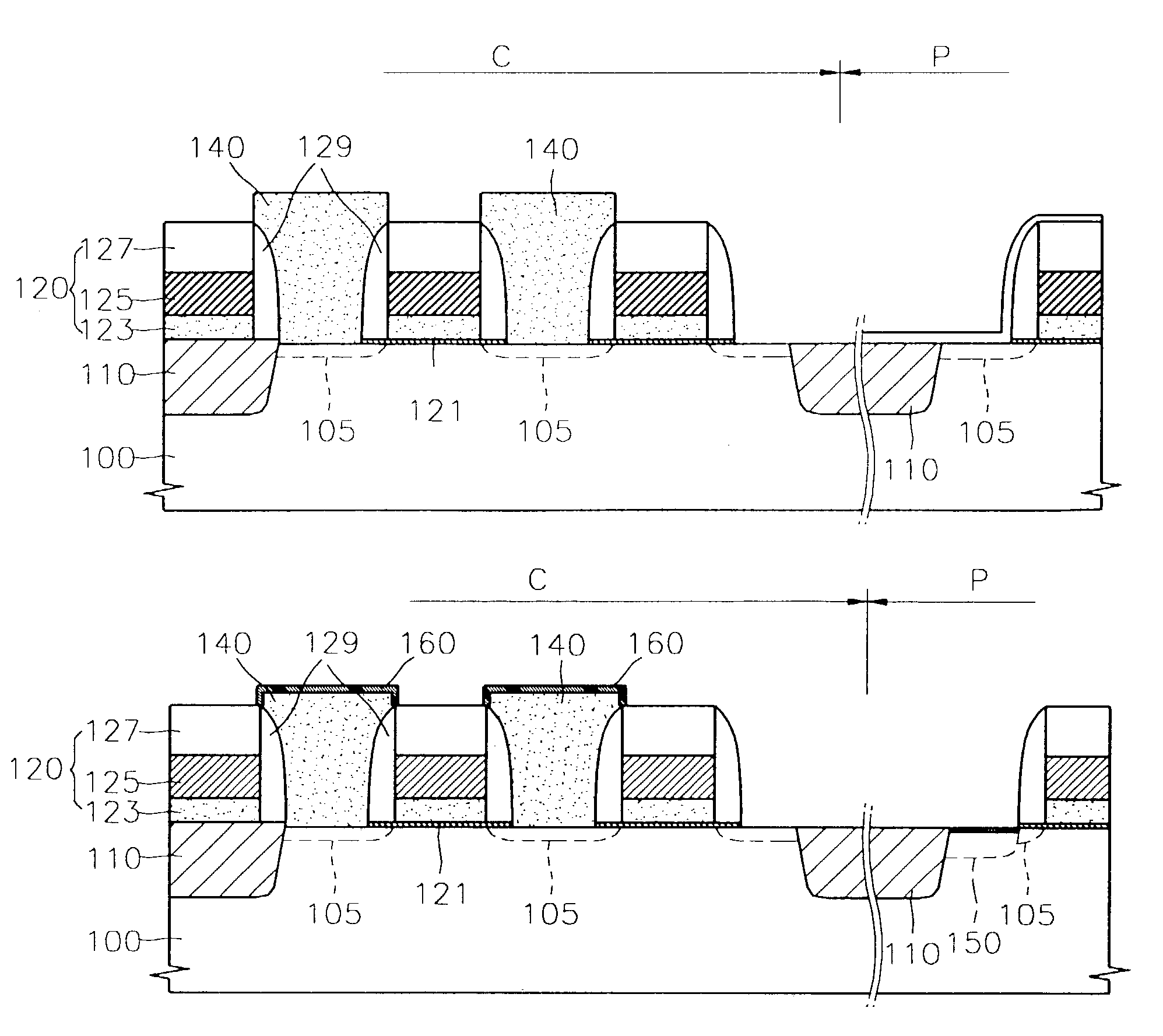
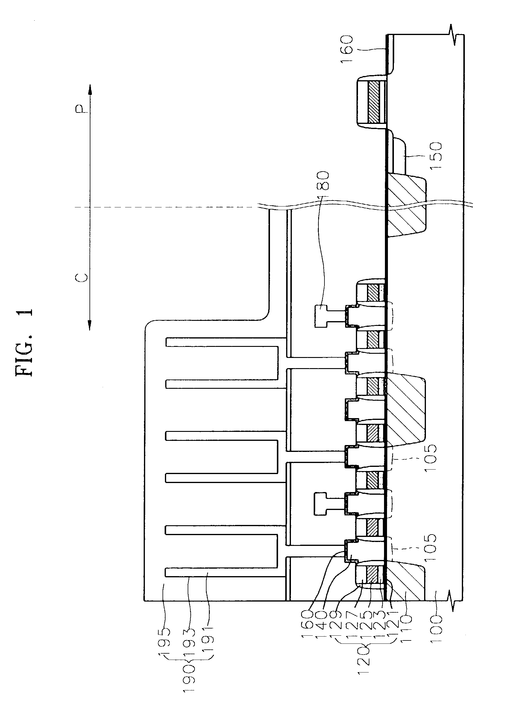
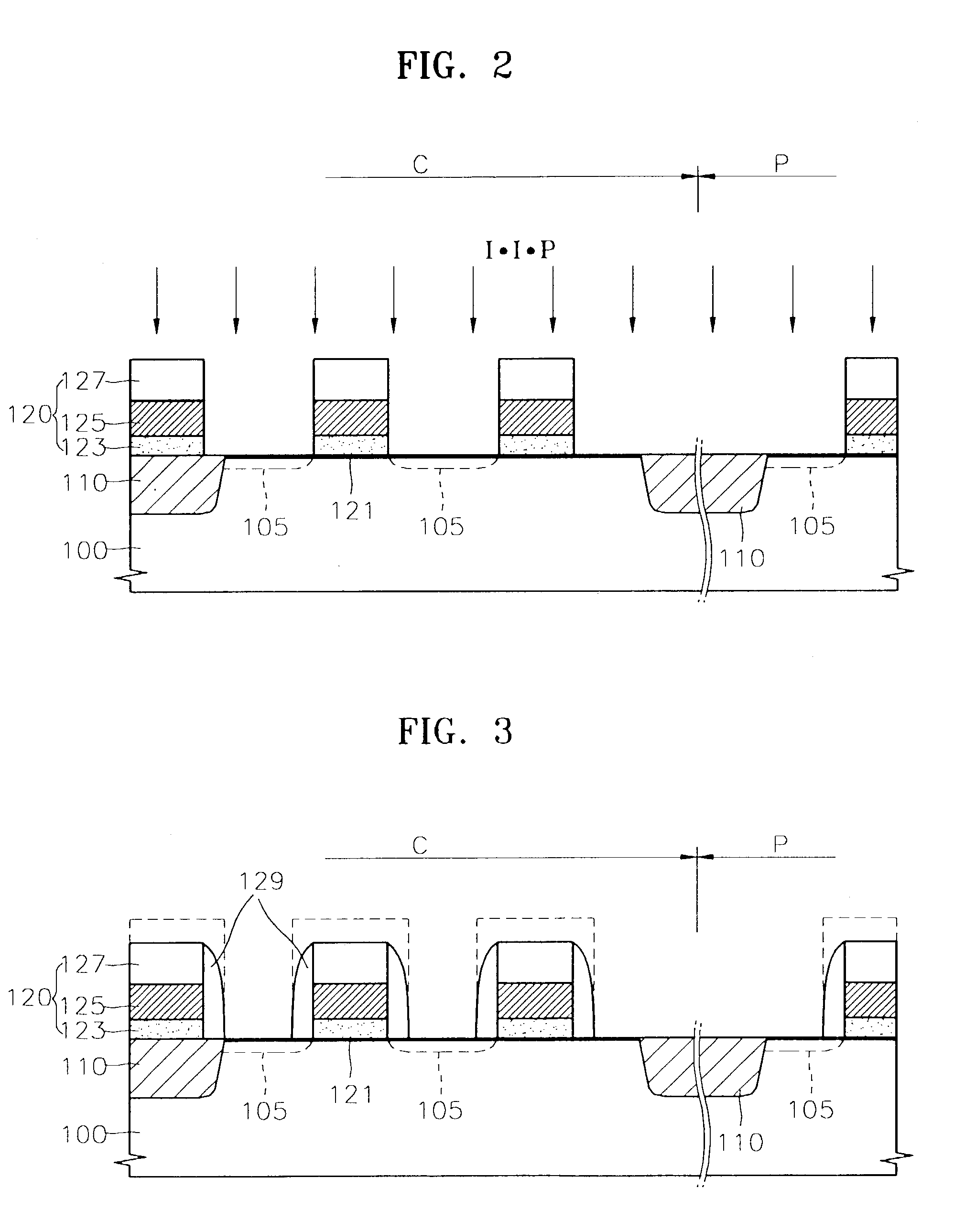
[0018]The present invention now will be described more fully hereinafter with reference to the accompanying drawings, in which various embodiments of the invention are shown. This invention may, however, be embodied in many different forms and should not be construed as limited to the embodiments set forth herein. Rather, these embodiments are provided so that this disclosure will be thorough and complete, and will fully convey the scope of the invention to those skilled in the art. In the drawings, the relative sizes and / or thicknesses of elements and / or layers may be exaggerated for clarity. When a layer is described as being on another layer or a semiconductor substrate, the layer may be directly on the other layer or semiconductor substrate, or other layers may be interposed therebetween. In contrast, when an element is referred to as being “directly on” another element, there are no intervening elements present. Like reference numerals in the drawings denote like members.

[0019]...


PUM


Abstract

An integrated circuit device having a semiconductor substrate includes a gate structure on the semiconductor substrate. Source/drain regions are on opposite sides of the gate structure. A contact pad is on at least one of the source/drain region, and a silicide cap is on a surface of the contact pad opposite the respective source/drain region.

Description

RELATED APPLICATIONS[0001]This application claims priority to Korean Patent Application No. 2002-46573, filed Aug. 7, 2002, in the Korean Intellectual Property Office, the disclosure of which is incorporated by reference herein in its entirety.BACKGROUND OF THE INVENTION[0002]1. Field of the Invention[0003]The present invention relates to a semiconductor devices and related methods, and more particularly, to contact pad configurations and related methods.[0004]2. Description of the Related Art[0005]As semiconductor devices become more highly integrated, many changes and improvements have been made in the structure of capacitors and bit lines of semiconductor memory devices. In 256M DRAMs or greater, contacts for the connection of a drain and a storage electrode used as a lower electrode of a capacitor and the connection of a source and a bit line are typically formed by the formation of contact pads through a self-aligned process.[0006]In such self-aligned formation of contacts and ...

Claims


Application Information

Patent Timeline
Patent Type & Authority Patents(United States)
IPC IPC(8): H01L21/44H01L21/20H01L21/8242H01L27/10H01L21/768H01L23/485H01L27/105H01L27/108
CPCH01L21/76885H01L21/76889H01L23/485H01L27/105H01L27/10817H01L27/10855H01L27/10888H01L27/10894H01L27/10897H01L2924/0002H01L2924/00H01L21/76897H10B12/318H10B12/485H10B12/09H10B12/50H10B12/0335H01L27/10
Inventor JANG, SE-MYEONGOH, YONG-CHULJIN, GYO-YOUNG
Owner SAMSUNG ELECTRONICS CO LTD
Why Eureka
Try Eureka