Light emitting diode and method of the same

a technology of light-emitting diodes and diodes, which is applied in the manufacture of semiconductor/solid-state devices, semiconductor devices, electrical apparatus, etc., can solve the problems of poor thermal dissipation and unsuitability for high-power applications, and achieve the effect of preventing static discharg

Active Publication Date: 2006-12-12
UNITED EPITAXY
View PDF6 Cites 21 Cited by
  • Summary
  • Abstract
  • Description
  • Claims
  • Application Information

AI Technical Summary

Benefits of technology

[0008]In one embodiment of the present invention, the light emitting diode includes a light emitting structure, a silicon substrate, and a bonding layer. The light emitting structure includes two semiconductor layers of different doped types. When a current passes through, the light emitting structure is capable of emitting light. The silicon substrate has two zones of different doped types. The bonding layer is interposed between the light emitting structure and the silicon substrate so that the semiconductor layer and the zone closest to the bonding layer are of different doped types. The bias applied on the light emitting structure in the present invention is a reverse bias with respect to the two zones of the silicon substrate so as to achieve the purpose of insulation. The two zones of the silicon substrate exhibit a Zener diode effect, which is capable of preventing static discharges.
[0012]Another aspect of the present invention is to provide a method of forming a light emitting diode. The method includes providing a light emitting structure including two semiconductor layers of different doped types. The light emitting structure is capable of emitting light when a current passes through. A silicon substrate having two zones of different doped types is also provided. By means of a bonding layer, the light emitting structure and the silicon substrate are bonded together so that the semiconductor layer and the zone closest to the bonding layer are of different doped types. The bias applied on the light emitting structure in the present invention is a reverse bias with respect to the two zones of the silicon substrate so as to achieve insulation purpose. The two zones of the silicon substrate exhibit a Zener diode effect, which is capable of preventing static discharges.

Problems solved by technology

High illumination light emitting diodes generally use GaAs substrates or sapphire substrates, which are poor in thermal dissipation and not suitable for high power applications.

Method used


Image

  • Light emitting diode and method of the same
  • Light emitting diode and method of the same
  • Light emitting diode and method of the same

Examples


Embodiment Construction

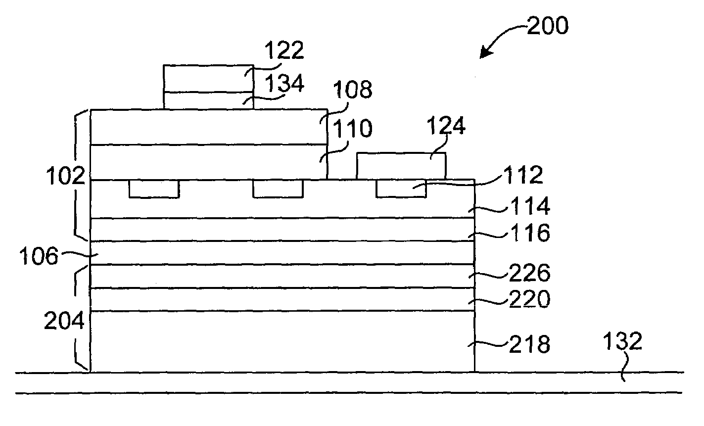
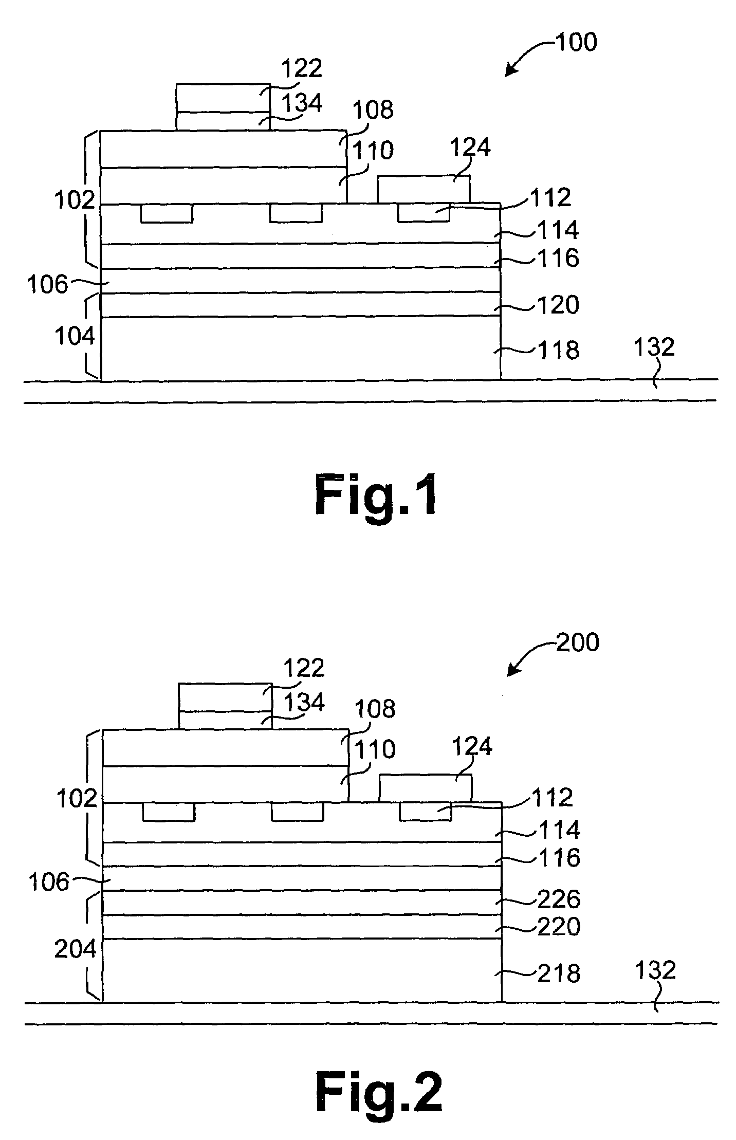
[0025]The present invention provides a light emitting diode, which is suitable for high current operation. FIGS. 1–7 illustrate preferred embodiments of the present invention. FIG. 1 illustrates a cross-sectional view of a light emitting diode 100 bonded to a base 132 in accordance with a first embodiment of the present invention. The light emitting diode 100 includes a light emitting structure 102, a silicon substrate 104, and a bonding layer 106. The light emitting structure 102 includes two semiconductor layers of different doped types, 108 and 110. The light emitting structure 102 is capable of emitting light when a current passes through. The silicon substrate 104 has two zones of different doped types, 118 and 120. The bonding layer 106 is interposed between the light emitting structure 102 and the silicon substrate 104 so that the semiconductor layer 110 and the zone 120 closest to the bonding layer 106 are of different doped types. It is noted that the bonding layer 106 is c...


PUM


Abstract

A light emitting diode and a method of the same are provided. The light emitting diode includes a light-emitting structure, a silicon substrate and a bonding layer. The light-emitting structure includes two semiconductor layers of different doped types. The light-emitting structure is capable of emitting light when a current passes through. The silicon substrate includes two zones of different doped types. The bonding layer is interposed between the light-emitting structure and the silicon substrate so that the semiconductor layer and the zone closest to the bonding layer are of different doped types.

Description

CROSS REFERENCE TO RELATED APPLICATIONS[0001]This application claims priority to Taiwan Patent Application No. 093112012 entitled “Light Emitting Diode and Method of the Same”, filed on Apr. 29, 2004, which is incorporated herein by reference and assigned to the assignee herein.FIELD OF INVENTION[0002]The present invention generally relates to a light emitting diode and a method of the same.BACKGROUND OF THE INVENTION[0003]High illumination light emitting diodes generally use GaAs substrates or sapphire substrates, which are poor in thermal dissipation and not suitable for high power applications. Conventionally, the light emitting structure formed on the GaAs substrate or the sapphire substrate is transferred onto a silicon substrate by wafer bonding technology, and then the GaAs or sapphire substrate is removed so as to solve the thermal dissipation problem.[0004]Horng et al. published an article entitled “AlGaInP light-emitting diodes with mirror substrates fabricated by wafer bo...

Claims


Application Information

Patent Timeline
Patent Type & Authority Patents(United States)
IPC IPC(8): H01L29/221H01L33/00H01L21/00
CPCH01L33/0079H01L33/0093
Inventor TU, CHUNG-CHENGLIN, JIN-YWAN
Owner UNITED EPITAXY
Why Eureka
Try Eureka