Insulated gate semiconductor device

a semiconductor device and gate technology, applied in the direction of semiconductor devices, basic electric elements, electrical equipment, etc., can solve the problems of large turn-on losses, inability to use conventional devices for gate driving, and loss of switching losses, so as to reduce di/dt, reduce turn-on losses and radiation noise, the effect of reducing di/d

Active Publication Date: 2006-12-19
FUJI ELECTRIC CO LTD
View PDF6 Cites 4 Cited by
  • Summary
  • Abstract
  • Description
  • Claims
  • Application Information

AI Technical Summary

Benefits of technology

[0020]According to the first aspect of the invention, the first main electrode contacts, in the vicinities of the runner disposed in the active region, with some of the semiconductor regions formed by dividing the third semiconductor layer, but not including any fourth semiconductor layer therein. This configuration facilitates reducing the gate-collector capacitance caused across the boundaries between the third semiconductor layer in the semiconductor regions not including any fourth semiconductor layer and the insulator films in the trenches and increasing the voltage drop speed and the current increase speed during the turn-on of the device. Therefore, the turn-on losses are reduced.
[0022]The semiconductor regions, formed by dividing the third semiconductor layer by the trenches and contacting only with the first main electrode electrically, and the semiconductor regions, formed by dividing the third semiconductor layer by the trenches and insulated from the first main electrode, are arranged appropriately so that the turn-on losses and the radiation noise may be reduced.
[0023]Advantageously, the number N1 of the some of the semiconductor regions, not including any fourth semiconductor layer but in contact with the first main electrode, and the number N2 of the other semiconductor regions, not including any fourth semiconductor layer but insulated from the first main electrode, are related with each other by the relational expression 0.25≦N1 / (N1+N2)≦0.75. By setting the numbers N1 and N2 such that these conditions are met, the turn-on losses and the radiation noise are reduced.
[0025]In the configuration described above, the first main electrode contacts with the third semiconductor layer only via the contact holes in the vicinities of the runner disposed in the active region and in the vicinities of the terminal ends of the trenches. This configuration facilitates reducing the gate-collector capacitance caused across the boundaries between the third semiconductor layer and the insulator films in the trenches and increasing the voltage drop speed and the current increase speed during the turn-on of the device. Therefore, the turn-on losses are reduced.
[0026]Advantageously, the number N1 of the second semiconductor regions and the number N2 of the third semiconductor regions are related with each other by the relational expression 0.25≦(N1 / (N1+N2)≦0.75. By setting the numbers N1 and N2 such that these conditions are satisfied, the turn-on losses and the radiation noise are reduced.
[0029]Since the above described advantageous configurations reduce di / dt by low gate resistance, the turn-on losses and the radiation noises are reduced. The insulated gate semiconductor device according to the invention facilitates reducing the turn-on losses and the radiation noises. Therefore, an insulated gate semiconductor device having a structure that meets the specifications for turn-on losses and radiation noise is obtained according to the invention.

Problems solved by technology

However, since the capacitance between the gate electrode and the emitter electrode, and the capacitance between the gate electrode and the collector electrode (hereinafter referred to as the “gate-collector capacitance”), are large, large switching losses are caused by the turning-on and turning-off of the trench IGBT.
Since the voltage drop speed and the current increase speed become slow in the turning-on of the trench IGBTs due to the large gate-collector capacitance, large turn-on losses are caused.
Therefore, it is impossible to use the conventional devices for gate driving.
Therefore, it is hard to reduce the radiation noises and the switching losses simultaneously.
Since a tradeoff exists between the turn-on losses and the radiation noise as described above, it is impossible for the trench IGBTs having any of the conventional structures to obtain an optimum structure that meets the specifications for turn-on losses and radiation noise.
It has been reported that the device characteristics exhibited by the IGBT turning on at a low current of about one-tenth the rated current greatly affects radiation noise (S. Momota, et al.
However, high gate resistance increases the turn-on losses of the IGBT. FIG. 11 is a wave chart describing the simulation results for comparing the turn-on characteristics of the IGBT shown in FIG. 8 and the conventional IGBTs with the gate resistance values thereof changed.
Although the gate resistance increase is preferable to reduce the radiation noise, switching losses increase, since the gate resistance increase causes long tails in the voltage waveforms.

Method used


Image

  • Insulated gate semiconductor device
  • Insulated gate semiconductor device
  • Insulated gate semiconductor device

Examples


first embodiment

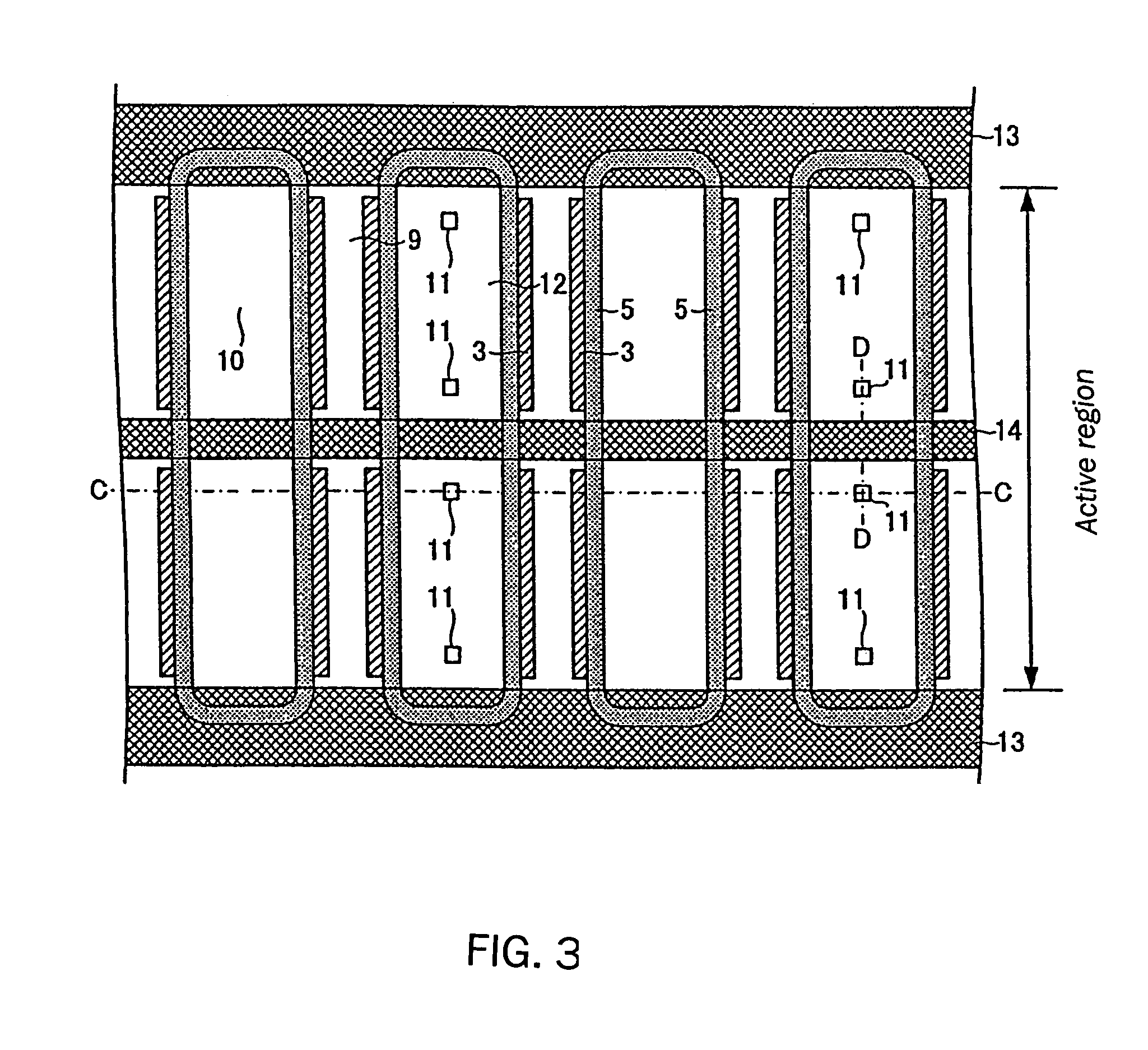
[0053]FIG. 3 is a top plan view schematically showing a trench IGBT according to a first embodiment of the invention. In FIG. 3, p-type base regions 9, 10, and 12, n-type source regions 3, gate electrodes 5, gate runners 13 and 14, and contact holes 11 projected to the surfaces of p-type base regions 12 are shown. Gate insulator films 4, interlayer insulator films 6, and emitter electrode 7 are not shown in FIG. 3.

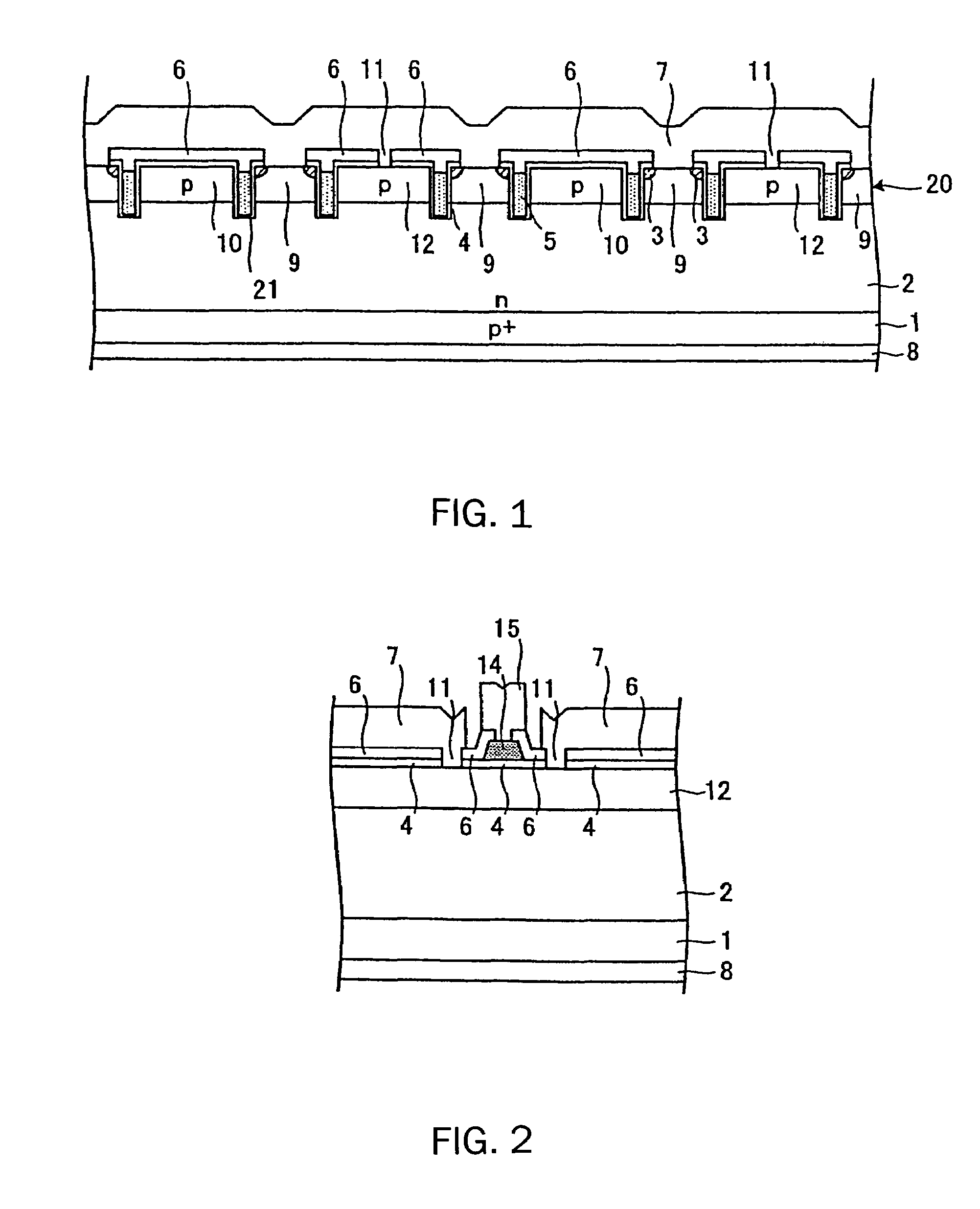
[0054]FIG. 1 is a cross-sectional view along the line segment C—C of FIG. 3 across n-type source regions 3, gate electrodes 5, and contact holes 11 in the vicinity of gate runner 14 in the active region. FIG. 2 is a cross sectional view along the line segment D—D of FIG. 3 across gate runner 14 in the active region and contact holes 11 on both sides of gate runner 14. In FIGS. 1 and 2, the constituent elements not shown in FIG. 3 are shown.

[0055]As shown in FIGS. 1 through 3, n-type drift layer 2 (a second semiconductor layer) is on p-type collector layer 1 (a first semico...

second embodiment

[0071]FIG. 6 is a top plan view schematically showing a trench IGBT according to a second embodiment of the invention. FIG. 7 is a cross sectional view along the line segment E—E of FIG. 6 across contact holes 11 aligned along a side of gate runner 14.

[0072]In the trench IGBT according to the first embodiment (shown in FIG. 1), n-type source regions 3 are formed only in first p-type base regions 9. To facilitate this, the position of the mask for forming n-type source regions 3 and the position of the mask for forming trenches 21 must be set very precisely relative to each other. In order to relax the required mask positioning precision and improve the mass-production efficiencies, it is effective to widen n-type source regions 3. In FIGS. 6 and 7, n-type source regions 3 are widened and formed on both sides of trenches 21. This configuration facilitates distributing n-type source regions 3 uniformly over the active region and reducing the complication of not forming n-type source r...

third embodiment

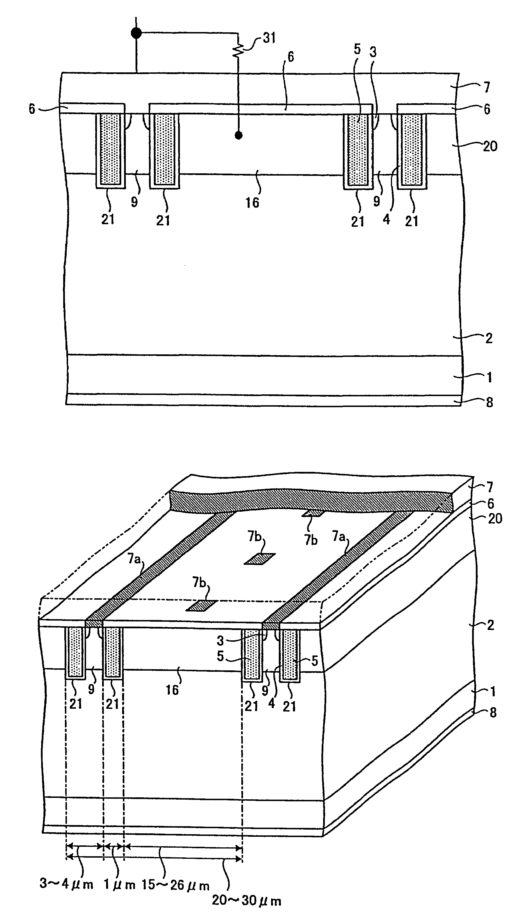
[0074]FIG. 8 is a cross sectional view for describing the principle of a trench IGBT according to a third embodiment of the invention. Referring now to FIG. 8, p-type base layer 20 is divided into relatively narrow p-type base regions 9 and relatively wide p-type base regions 16 wider than relatively narrow p-type base regions 9. Relatively wide p-type base region 16 is connected electrically to emitter electrode 7 via gate resistance 31 of 50 mΩ or higher. Emitter electrode 7 is in contact commonly with n-type source regions 3 (in relatively narrow p-type base regions 9) and relatively narrow p-type base region 9 in the same manner as in the trench IGBT according to the first embodiment.

[0075]FIG. 9 is a graph describing the simulated relation between the peak current reduction rate and the value of gate resistance 31 in the trench IGBT having the structure shown in FIG. 8. When the peak current value in the structure which insulates relatively wide p-type base regions 16 from emit...


PUM


Abstract

A trench IGBT is disclosed which meets the specifications for turn-on losses and radiation noise. It includes a p-type base layer divided into different p-type base regions by trenches. N-type source regions are formed in only some of the p-type base regions. There is a gate runner in the active region of the trench IGBT. Contact holes formed in the vicinities of the terminal ends of the trenches and on both sides of the gate runner electrically connect some of the p-type base regions that do not include source regions to an emitter electrode. The number N1 of p-type base regions that are connected electrically to the emitter electrode and the number N2 of p-type base regions that are insulated from the emitter electrode are related with each other by the expression 25≦{N1 / (N1+N2)}×100≦75.

Description

CROSS REFERENCE TO RELATED APPLICATIONS[0001]This application claims priority from application Serial No. JP 2003-390433 filed on Nov. 20, 2003 and JP 2004-224777, filed on Jul. 30, 2004, and the contents of these two documents are incorporated herein by reference in their entirety.BACKGROUND OF THE INVENTION[0002]A. Field of the Invention[0003]The present invention relates generally to insulated gate semiconductor devices and, more particularly, to trench-type insulated gate bipolar transistors (hereinafter referred to as “trench IGBTs”), which include an insulated gate structure in the trenches formed in a semiconductor substrate.[0004]B. Description of the Related Art[0005]Recently, trench IGBTs have been attracting much attention in the field of power devices used for electric power converters. Since the trench IGBT facilitates increased trench density, the voltage drop VCE(sat) in the ON-state of the trench IGBT is small and the steady state losses are reduced. However, since t...

Claims


Application Information

Patent Timeline
Patent Type & Authority Patents(United States)
IPC IPC(8): H01L29/76H01L29/94H01L31/062H01L31/113H01L31/119H01L29/06H01L29/78H01L29/739
CPCH01L29/0696H01L29/7397
Inventor WAKIMOTO, HIROKIMOMOTA, SEIJIOTSUKI, MASAHITO
Owner FUJI ELECTRIC CO LTD
Why Eureka
Try Eureka