Method of exposing using electron beam

a technology of electron beam and electron beam, which is applied in the direction of beam/ray deflecting arrangement, optical radiation measurement, particle separator tubes, etc., can solve the problems of deteriorating numerical accuracy and precision of patterns, distorted patterns, and scattered electrons becoming obstacles, so as to improve the proximity effect and the generation of heat, accuracy and the effect of pattern accuracy

Active Publication Date: 2006-12-26
SAMSUNG ELECTRONICS CO LTD
View PDF4 Cites 0 Cited by
  • Summary
  • Abstract
  • Description
  • Claims
  • Application Information

AI Technical Summary

Benefits of technology

[0018]The present invention provides a method of exposing using an electron beam for improving numerical accuracy and precision between an initial designed pattern and a pattern, which is obtained by exposing, and for realizing the pattern having desired shape and structure, by removing a proximity effect and a heat generation problem that occur due to an electron scattering.
[0032]The method of exposing using the electron beam according to the present invention can improve a proximity effect and the generation of heat by an electron scattering when patterning a photosensitive layer into a predetermined shape by using the electron beam. Thus, the accuracy and the precision of the patterns may be secured. In addition, the method of exposing using the electron beam according to the present invention may be applied to various equipments of exposing using an electron beam. Furthermore, the method of exposing using the electron beam can precisely form fine and complicated patterns, thus the method can realize fine patterns of various shapes.

Problems solved by technology

Here, such scattered electrons become obstacles when realizing fine patterns.
As a result, the exposing characteristic of the photosensitive layer is changed, thus the pattern may be distorted.
In other words, the numerical accuracy and precision of the pattern are deteriorated.
In addition, the software program only compensates the size of the exposure pattern, and it is required to process a large amount of data to calculate a process shift amount for a portion deviated from the size of the exposure pattern.
Furthermore, the software program cannot remove the proximity effect from a complicated pattern and an entire area of the pattern.

Method used


Image

  • Method of exposing using electron beam
  • Method of exposing using electron beam
  • Method of exposing using electron beam

Examples


first embodiment

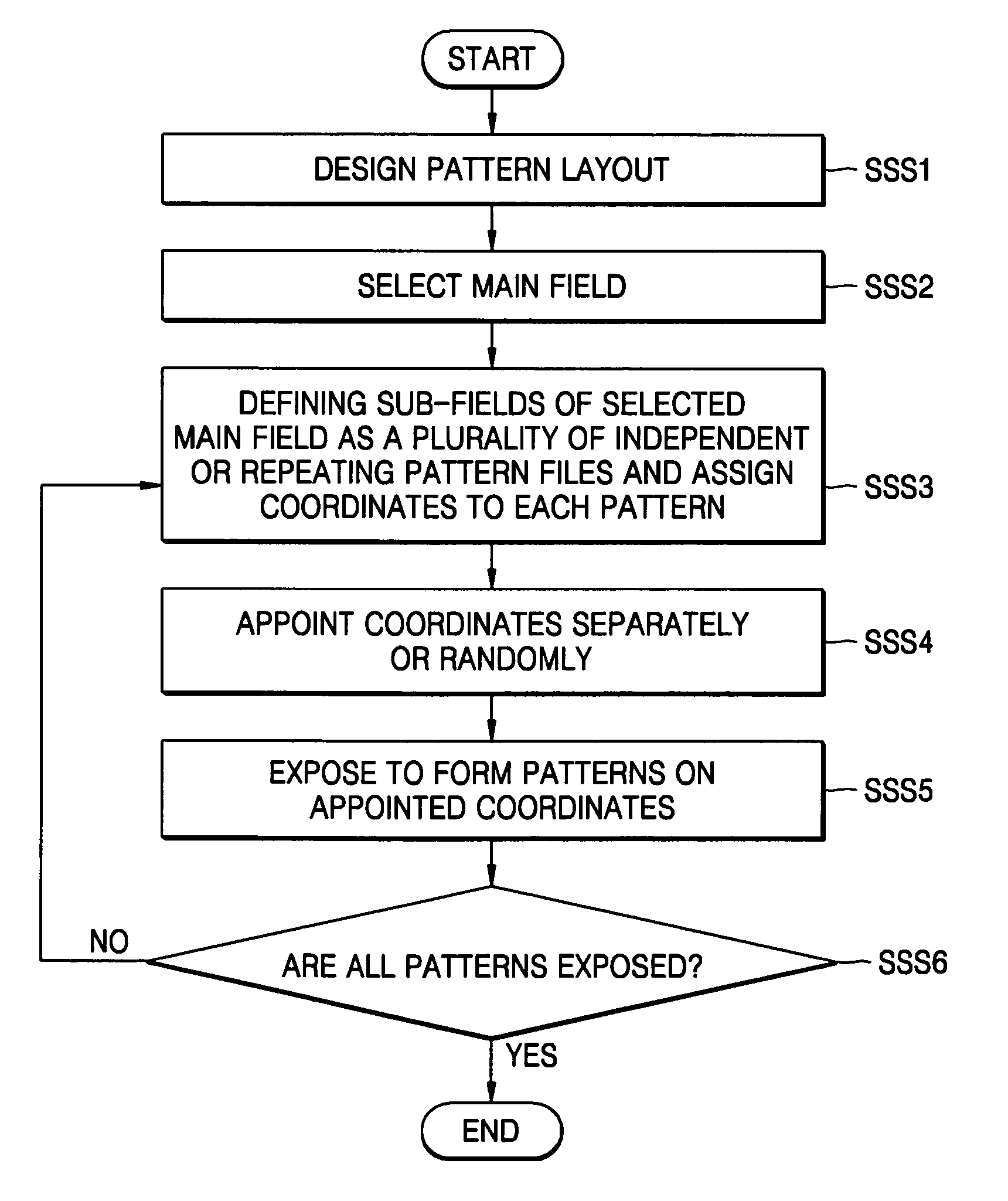
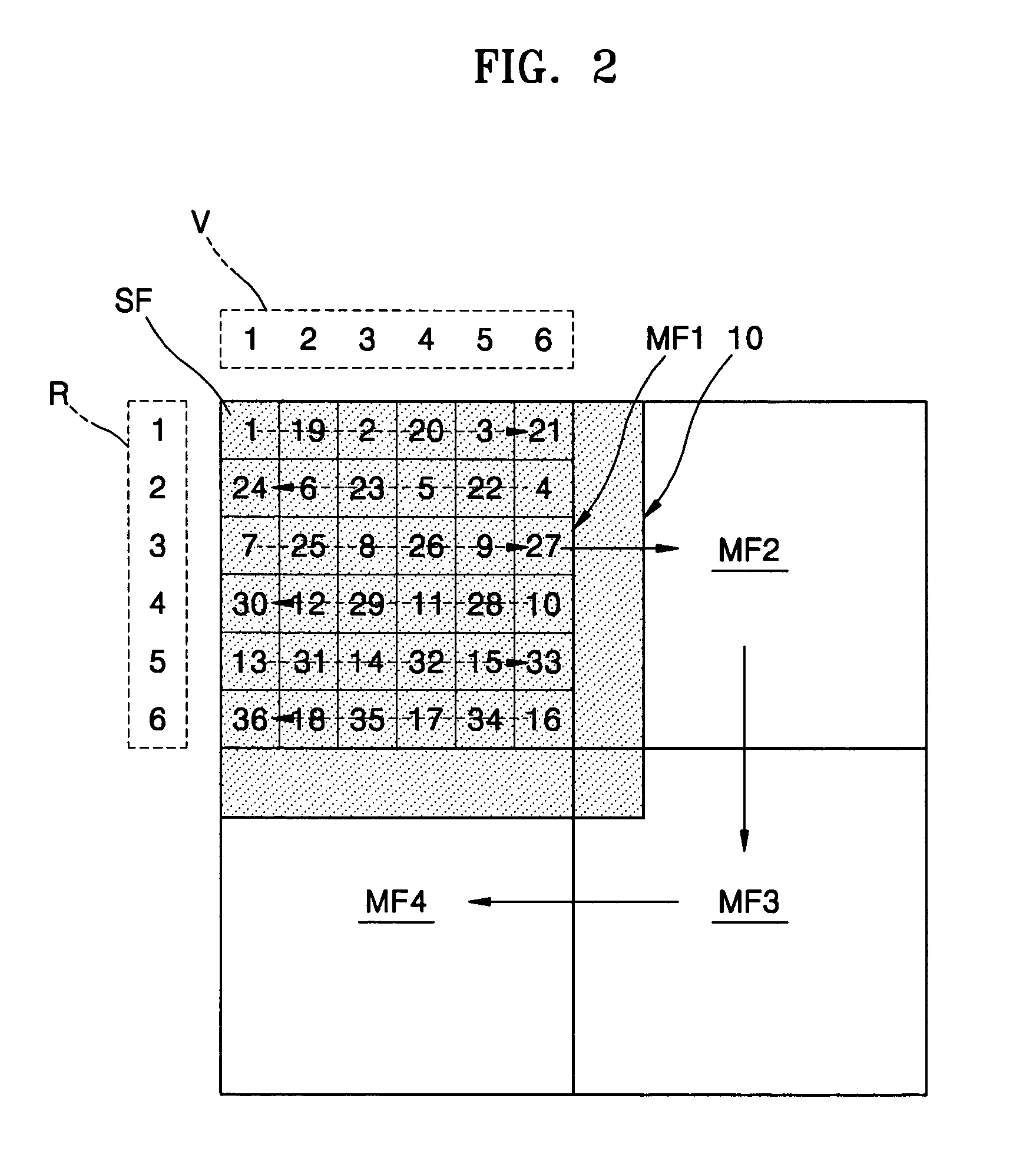
[0043]A method of exposing using an electron beam according to the present invention will now be described with reference to FIG. 2.

[0044]Referring to FIG. 2, a specimen or a photosensitive layer 10 to be exposed is divided into first through fourth main fields MF1, MF2, MF3, and MF4. Here, the number of the main fields can vary based on the area to be exposed. For example, in the case of the photosensitive layer 10 is smaller than the first main field MF1, first main field MF1 is enough for the photosensitive layer 10. On the contrary, in the case of the photosensitive layer 10 is larger than the size of the first through fourth main fields MF1 through MF4, the number of fields more than four are required for the photosensitive layer 10. Exposing processes on the first through fourth main fields MF1 through MF4 are the same except exposure area. Thus, only the description of the exposure of the first main field MF1 is described below and descriptions of the exposure of the second t...

second embodiment

[0052]A method of exposing using an electron beam according to the present invention will now be described.

[0053]In the method of exposing using the electron beam according to the second embodiment of the present invention, each row is exposed in the same direction.

[0054]More specifically, in the first exposing method according to the present invention, the exposure direction of the first, third, and fifth rows is opposite to the exposure direction of the other rows.

[0055]However, in the method of exposing using the electron beam according to the second embodiment of the present invention that will be referred to as a second exposing method according to the present invention, the exposure direction is the same for every row while skipping one sub-field for each sub-field.

[0056]The second exposing method according to the present invention can be clear by referring numbers marked on the sub-fields SF of FIG. 3.

[0057]Specifically, after exposing sub-fields located at (1, 1), (1, 3), an...

third embodiment

[0062]A method of exposing using an electron beam according to the present invention will now be described.

[0063]In the method of exposing using the electron beam according to the third embodiment, sub-fields to be exposed are randomly selected while preventing adjacent sub-fields from being selected and one sub-field from being selected repeatedly.

[0064]In other words, the method of exposing according to the third embodiment of the present invention that will be referred to as a third exposing method according to the present invention randomly selects the sub-fields to be exposed.

[0065]The random selection of the sub-fields can be possible by programming an equipment for exposing using an electron beam. By the programming, random numbers are generated using meshing and grouping and the sub-fields corresponding to the random numbers are exposed. Here, it is not preferable that the adjacent sub-fields are sequentially selected and one sub-field are repeatedly selected.

[0066]Thus, any...


PUM


Abstract

Provided is a method of exposing using an electron beam. The provided method of exposing using the electron beam includes defining main fields on an exposure area of an electron beam exposure target and defining a plurality of sub-fields on the main fields, selecting a main field to be exposed, selecting at least one sub-field of the selected main field, exposing the selected sub-field by using the electron beam, and selecting at least one of the other sub-field, which is not adjacent to the previously selected sub-field and not exposed yet, and exposing the sub-field by using the electron beam.

Description

BACKGROUND OF THE INVENTION[0001]This application claims the priority of Korean Patent Application No. 10-2004-0012536, filed on Feb. 25, 2004, in the Korean Intellectual Property Office, the disclosure of which is incorporated herein in its entirety by reference.[0002]1. Field of the Invention[0003]The present invention relates to a method of manufacturing a semiconductor device, and more particularly, to a method of exposing using an electron beam.[0004]2. Description of the Related Art[0005]Along with the development of a technology of manufacturing a semiconductor device, an equipment for manufacturing a semiconductor device is also improved. An example of the equipment for manufacturing a semiconductor device is an equipment for exposing using an electron beam. Nowadays, equipments of adopting various methods of exposing are introduced to improve productivity.[0006]Examples of the introduced equipments include an equipment for changing the spot size of electron beams during an ...

Claims


Application Information

Patent Timeline
Patent Type & Authority Patents(United States)
IPC IPC(8): H01J37/08H01L21/027
CPCB82Y10/00B82Y40/00H01J37/3026H01J37/3174Y10S430/143B41F17/36B41F31/20
Inventor KIM, HAE-SUNGLEE, MYUNG-BOKSOHN, JIN-SEUNGJUNG, MEE-SUKCHO, EUN-HYOUNG
Owner SAMSUNG ELECTRONICS CO LTD
Why Eureka
Try Eureka