Circuit and method for adding parametric test capability to digital boundary scan

a parametric test and digital boundary scan technology, applied in the direction of electronic circuit testing, measurement devices, instruments, etc., can solve the problems of increasing the cost of high-pin-count testers, becoming more difficult to quickly diagnose and repair boards,

Active Publication Date: 2007-01-02
SIEMENS PROD LIFECYCLE MANAGEMENT SOFTWARE INC
View PDF13 Cites 27 Cited by
  • Summary
  • Abstract
  • Description
  • Claims
  • Application Information

AI Technical Summary

Benefits of technology

[0018]The present invention also seeks to provide test circuitry which will permit sequential analog access to the digital and analog pins without requiring reloading of the boundary scan chain, and the digital result of a sequential comparison between each pin's voltage and a reference voltage be output via the TDO pin so that commonly available 1149.1-based board test equipment can monitor the comparison results.

Problems solved by technology

As printed circuit boards populated with ICs get smaller and more dense, it becomes more difficult to quickly diagnose and repair the boards.
Further, as the pin-count of new ICs increases each year, and the cost of high pin-count testers increases, it becomes necessary to consider reduced pin count testing where only a small subset of an IC's pins are contacted during an IC test.
A drawback of existing circuits is that a designer who wishes to provide analog access to digital IC pins that are controlled by 1149.1 boundary scan, is compelled to use the 1149.4 boundary scan cells of FIG. 4, and accept the accompanying gate count penalty, in order to use conventional 1149.1 and 1149.4 software and hardware tools for performing boundary scan testing.

Method used


Image

  • Circuit and method for adding parametric test capability to digital boundary scan
  • Circuit and method for adding parametric test capability to digital boundary scan
  • Circuit and method for adding parametric test capability to digital boundary scan

Examples


Embodiment Construction

[0043]In the following detailed description, numerous specific details are set forth in order to provide a thorough understanding of the present invention. However, it will be understood by those skilled in the art that the present invention may be practiced without these specific details. In other instances, well known methods, procedures, components and circuits have not been described in detail so as not to obscure aspects of the present invention.

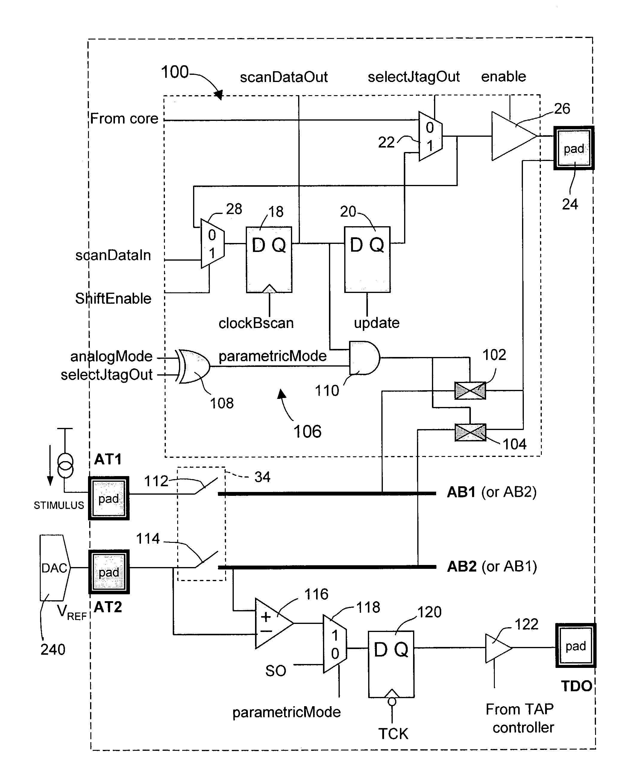
[0044]A primary objective of the invention is to facilitate analog access to digital IC pins that are controlled by 1149.1 boundary scan cells in a way that is compliant with 1149.4 but that uses fewer logic gates than 1149.4 requires for analog pins.

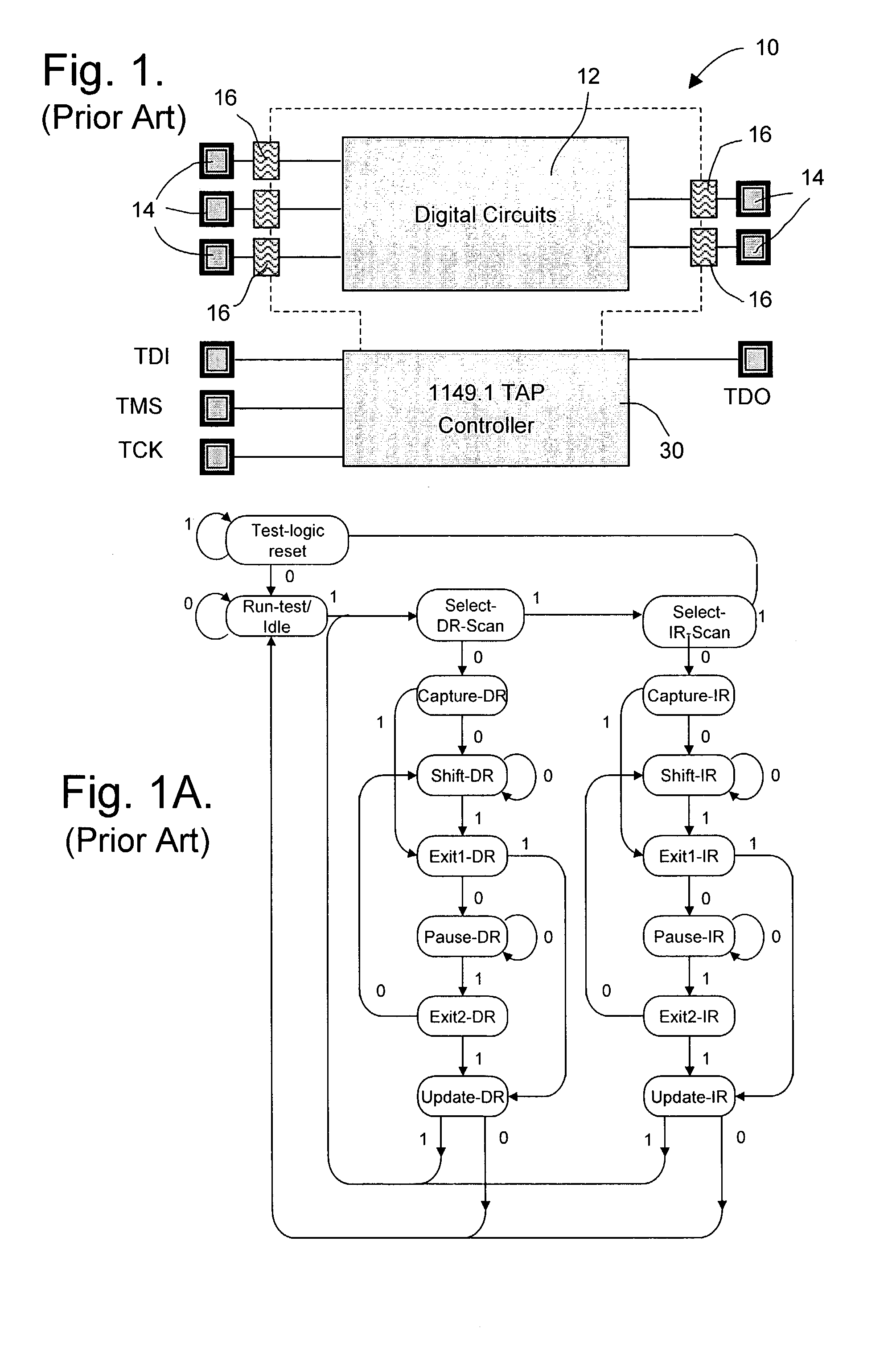
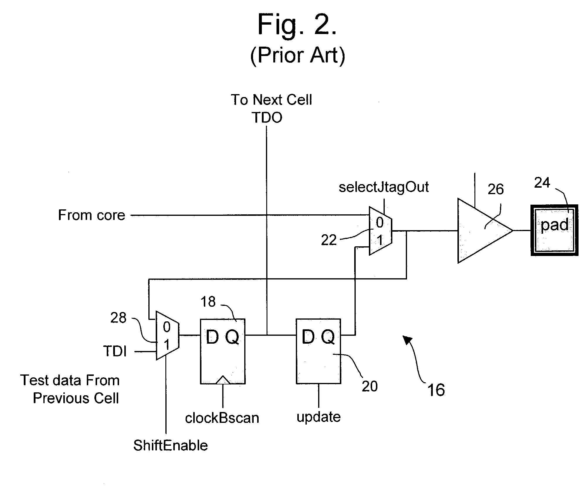
[0045]As previously mentioned, 1149.4 defines an analog bus that connects within each IC to the pins of the IC and permits an analog stimulus current to be conveyed to each pin on a bus, AB1, and the analog response voltage to be conveyed from each pin on another bus, AB2, as shown in FIG. ...


PUM


Abstract

A boundary scan cell for use in a circuit having a boundary scan shift register (BSSR) having boundary scan cells associated with pins of the circuit, the cell having a single-bit shift register element and an associated update latch, comprises a logic circuit for controlling the logic state of an associated pin, analog switches connecting the associated pin to analog test buses, and logic circuitry for selectively configuring the cell in a parametric test mode in which the cell shift register element controls the analog switches, and in a digital test mode in which the cell shift register element controls the logic state of the associated pin.

Description

CROSS-REFERENCE TO RELATED APPLICATIONS[0001]This application claims the benefit of U.S. Provisional Patent Application Ser. No. 60 / 376,557 filed May 1, 2002.BACKGROUND OF THE INVENTION[0002]1. Field of the Invention[0003]The present invention generally relates to the testing of integrated circuits (ICs) and circuit boards, or substrates, on which ICs are mounted and, more specifically, to a logic circuit for a circuit boundary scan cell and a method for performing parametric tests on a circuit having digital and analog pins.[0004]2. Description of Related Art[0005]As printed circuit boards populated with ICs get smaller and more dense, it becomes more difficult to quickly diagnose and repair the boards. As a result, digital boundary scan is becoming a popular design for test (DFT) technique to permit quick verification of board-level connections between ICs. Further, as the pin-count of new ICs increases each year, and the cost of high pin-count testers increases, it becomes necess...

Claims


Application Information

Patent Timeline
Patent Type & Authority Patents(United States)
IPC IPC(8): G01R31/28G01R31/30G01R31/3185
CPCG01R31/3012G01R31/318533G01R31/3167
Inventor SUNTER, STEPHEN K.
Owner SIEMENS PROD LIFECYCLE MANAGEMENT SOFTWARE INC
Why Eureka
Try Eureka