Techniques for reducing bowing in power transistor devices

a technology of power transistors and bowing, which is applied in the direction of semiconductor devices, semiconductor/solid-state device details, electrical apparatus, etc., can solve the problems of difficult to pick up, place and attach the bowed device with a uniform and planar bondline, and the bowed device is often prone to bowing, so as to reduce the amount of bowing

Active Publication Date: 2007-01-16
BELL SEMICON LLC
View PDF14 Cites 7 Cited by
  • Summary
  • Abstract
  • Description
  • Claims
  • Application Information

AI Technical Summary

Benefits of technology

[0007]The present invention provides power transistor devices and techniques for reducing bowing in such devices. In one aspect of the invention, a power transistor device is provided. The power transistor device comprises a substrate, a device film formed on the substrate and an adhesion layer formed on a side of the substrate opposite the device film, wherein at least a portion of the adhesion layer is at least partially segmented. The power transistor device thereby exhibits a reduced amount of bowing relative to an amount of bowing expected without the segmenting of the adhesion layer. The power transistor device may be part of an integrated circuit.
[0008]In another aspect of the invention, a method of processing a power transistor device is provided. In the method, a device film is formed on a substrate, an adhesion layer is formed on a side of the substrate opposite the device film, and at least a portion of the adhesion layer is at least partially segmented. The power transistor device thereby exhibits a reduced amount of bowing relative to an amount of bowing expected without the segmenting of the adhesion layer.

Problems solved by technology

However, due to the thinning of the substrate and to stresses associated with device components, bowing of the device often occurs.
Bowing presents an issue for handling and attaching the device, e.g., to the heat sink.
More specifically, a bowed device is difficult to pick up, place and attach with a uniform and planar bondline.
However, these metals, and Ti in particular, have high inherent stresses that only add to the bowing of the device.
Bowing of the device may cause voids to form between the device and the heat sink, resulting in an unfavorable and non-uniform mating of surfaces, and thus inadequate heat removal characteristics.

Method used


Image

  • Techniques for reducing bowing in power transistor devices
  • Techniques for reducing bowing in power transistor devices
  • Techniques for reducing bowing in power transistor devices

Examples


Embodiment Construction

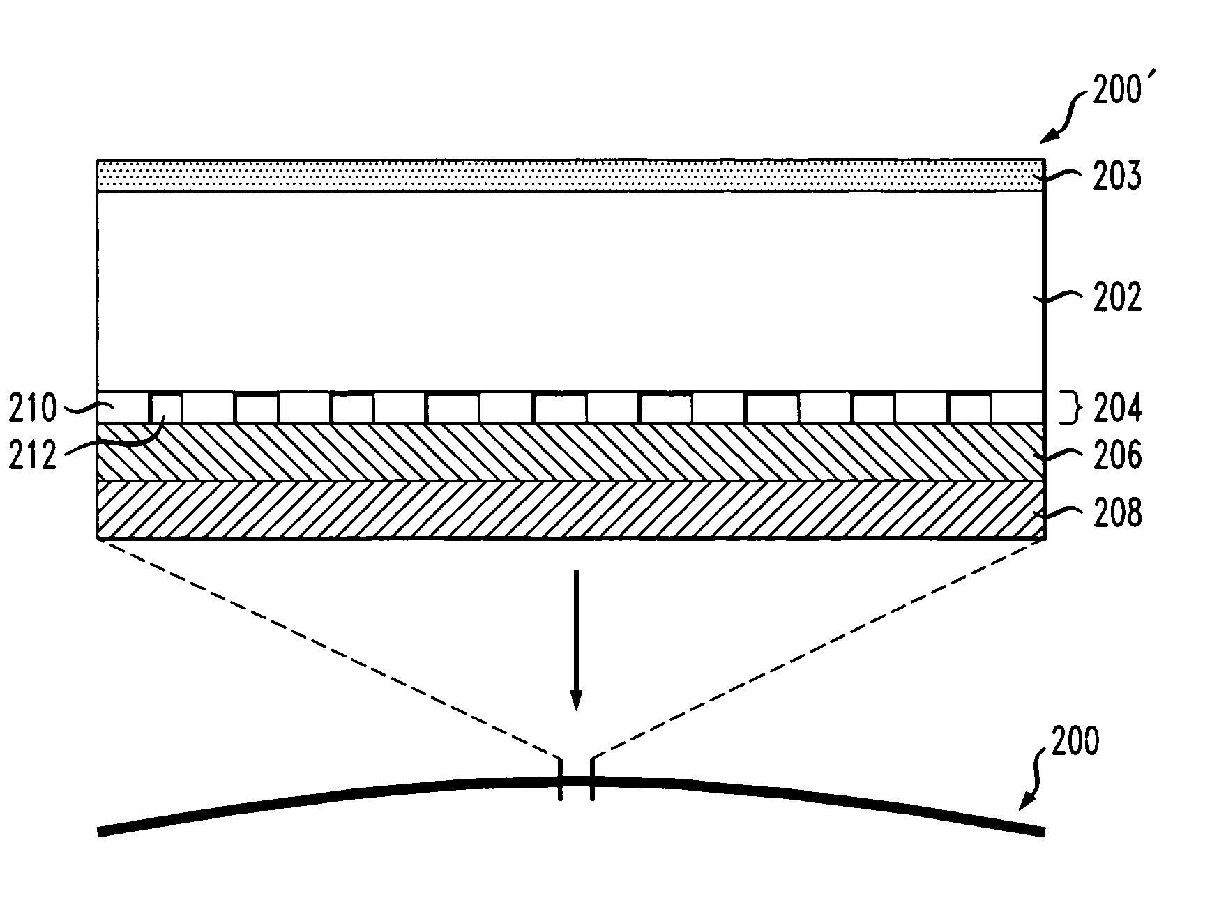
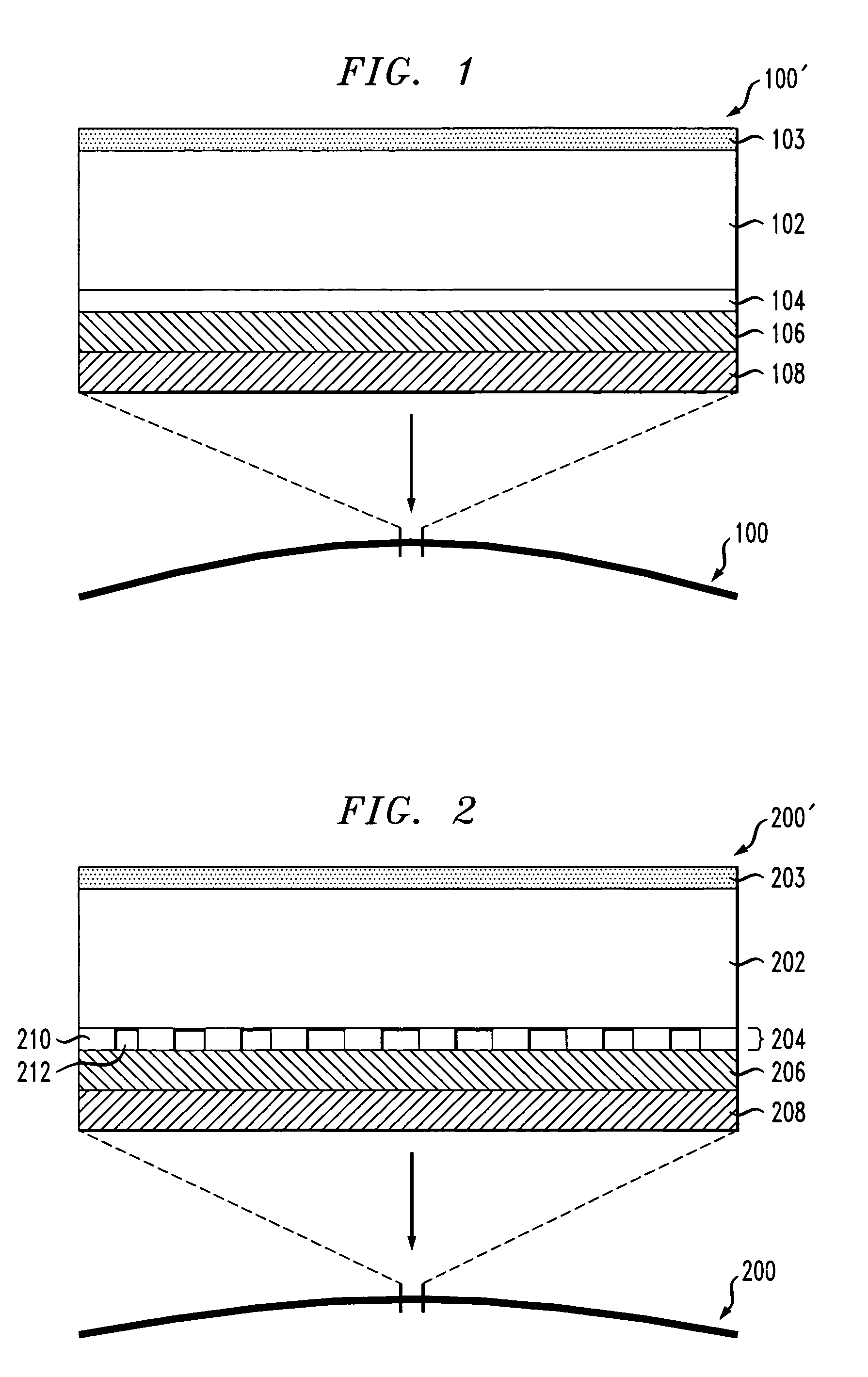
[0013]FIG. 1 illustrates one possible power transistor device configuration, namely a power transistor device having a blanket adhesion layer. In FIG. 1, a cross-section 100′ of power transistor device 100 comprises device film 103, substrate 102 and blanket adhesion layer 104. As shown in FIG. 1, power transistor device 100 may also comprise additional metal layers, e.g., metal layers 106 and 108 which may be implemented, for example, in attaching power transistor device 100, e.g., by soldering to a metal heat sink.

[0014]For example, metal layer 106 may comprise a barrier material that prevents any species present in blanket adhesion layer 104 from migrating into, e.g., metal layer 108. Metal layer 108 may comprise a wettable material compatible with soldering attachment techniques. Accordingly, metal layer 106, when comprising a barrier material, can prevent blanket adhesion layer 104 species from migrating into and contaminating the wettable material of metal layer 108. As is des...


PUM


Abstract

Power transistor devices and techniques for reducing bowing in such devices are provided. In one aspect, a power transistor device is provided. The power transistor device comprises a substrate, a device film formed on the substrate and an adhesion layer formed on a side of the substrate opposite the device film, wherein at least a portion of the adhesion layer is at least partially segmented. The power transistor device thereby exhibits a reduced amount of bowing relative to an amount of bowing expected without the segmenting of the adhesion layer. The power transistor device may be part of an integrated circuit.

Description

CROSS-REFERENCE TO RELATED APPLICATIONS[0001]The present invention is related to U.S. patent application Ser. No. 10 / 628,941, filed on Jul. 29, 2003, and entitled “Techniques for Curvature Control in Power Transistor Devices,” the disclosure of which is hereby incorporated by reference.FIELD OF THE INVENTION[0002]The present invention relates generally to power transistor devices, and more particularly to techniques for reducing bowing experienced in such devices.BACKGROUND OF THE INVENTION[0003]Power transistor devices, e.g., radio frequency (RF) power transistors, operate at a high junction temperature. It is desirable for power transistor device assemblies to have a high thermal conductivity for proper performance and reliability. Thus, efforts are made during the processing of such power transistor devices to ensure that proper thermal coupling exists between a given device and a heat sink upon which the device is typically mounted, so that sufficient heat removal is attained.[0...

Claims


Application Information

Patent Timeline
Patent Type & Authority Patents(United States)
IPC IPC(8): H01L23/10H01L23/34H01L21/331H01L29/00H01L29/06
CPCH01L29/66234H01L29/0657
Inventor BRENNAN, JOHN MCKENNAFREUND, JOSEPH MICHAELOSENBACH, JOHN WILLIAM
Owner BELL SEMICON LLC
Why Eureka
Try Eureka