Integrated circuit devices with an auxiliary pad for contact hole alignment

a technology of integrated circuits and contact holes, which is applied in the direction of semiconductor devices, semiconductor/solid-state device details, electrical apparatus, etc., can solve the problems of increasing the difficulty of forming properly aligned contact holes therewith, voids may occur, and small contact hole areas are difficult to fill, etc., to achieve the effect of simplifying subsequent processes, simplifying alignment of photoresist mask patterns, and high integration density

Inactive Publication Date: 2007-01-16
SAMSUNG ELECTRONICS CO LTD
View PDF31 Cites 0 Cited by
  • Summary
  • Abstract
  • Description
  • Claims
  • Application Information

AI Technical Summary

Benefits of technology

[0009]The contact hole or via hole can be sufficiently large to expose both the conductive pad and the auxiliary pad. To enable high integration density, the auxiliary pad 54b can be formed close to the conductive pad 54a so that it is substantially exposed by the contact hole 58. Exposing the auxiliary pad 54b with the contact pad 54a can enable the contact hole 58 to be substantially larger than the contact pad 54a alone and simplify alignment of a photoresist mask pattern which is used to form the contact hole 58. A larger contact hole provides an increased contact area which in-turn can simplify subsequent processes for filling of the contact hole, such as with an upper wiring, and avoid voids within the contact hole.
[0010]The effect of misalignment when the contact hole or via hole is formed can be reduced by forming the auxiliary pad adjacent to and electrically isolated from the contact pad. In particular, the hole can be larger which can simplify alignment of a mask for forming the hole. Moreover, a larger hole can provide an increased contact area which in-turn can simplify subsequent processes for filling the hole without voids.

Problems solved by technology

Decreased widths of the metal wiring and contact pads can considerably increase the difficulty of forming a properly aligned contact hole therewith.
Moreover, small contact hole areas can be difficult to fill with a conductive layer and a void may occur in the contact hole.

Method used


Image

  • Integrated circuit devices with an auxiliary pad for contact hole alignment
  • Integrated circuit devices with an auxiliary pad for contact hole alignment
  • Integrated circuit devices with an auxiliary pad for contact hole alignment

Examples


Embodiment Construction

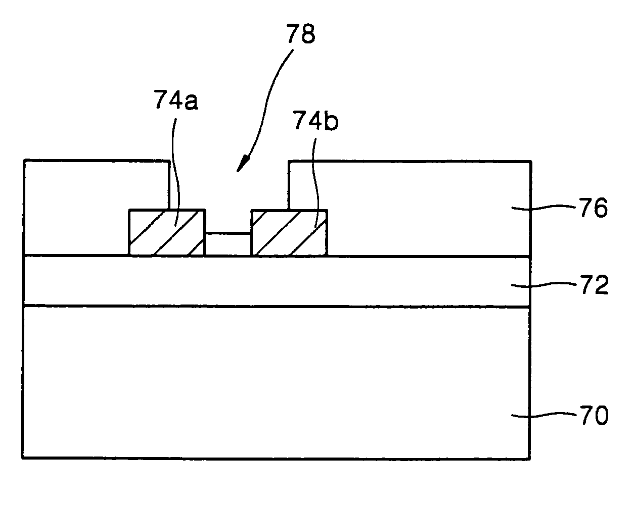
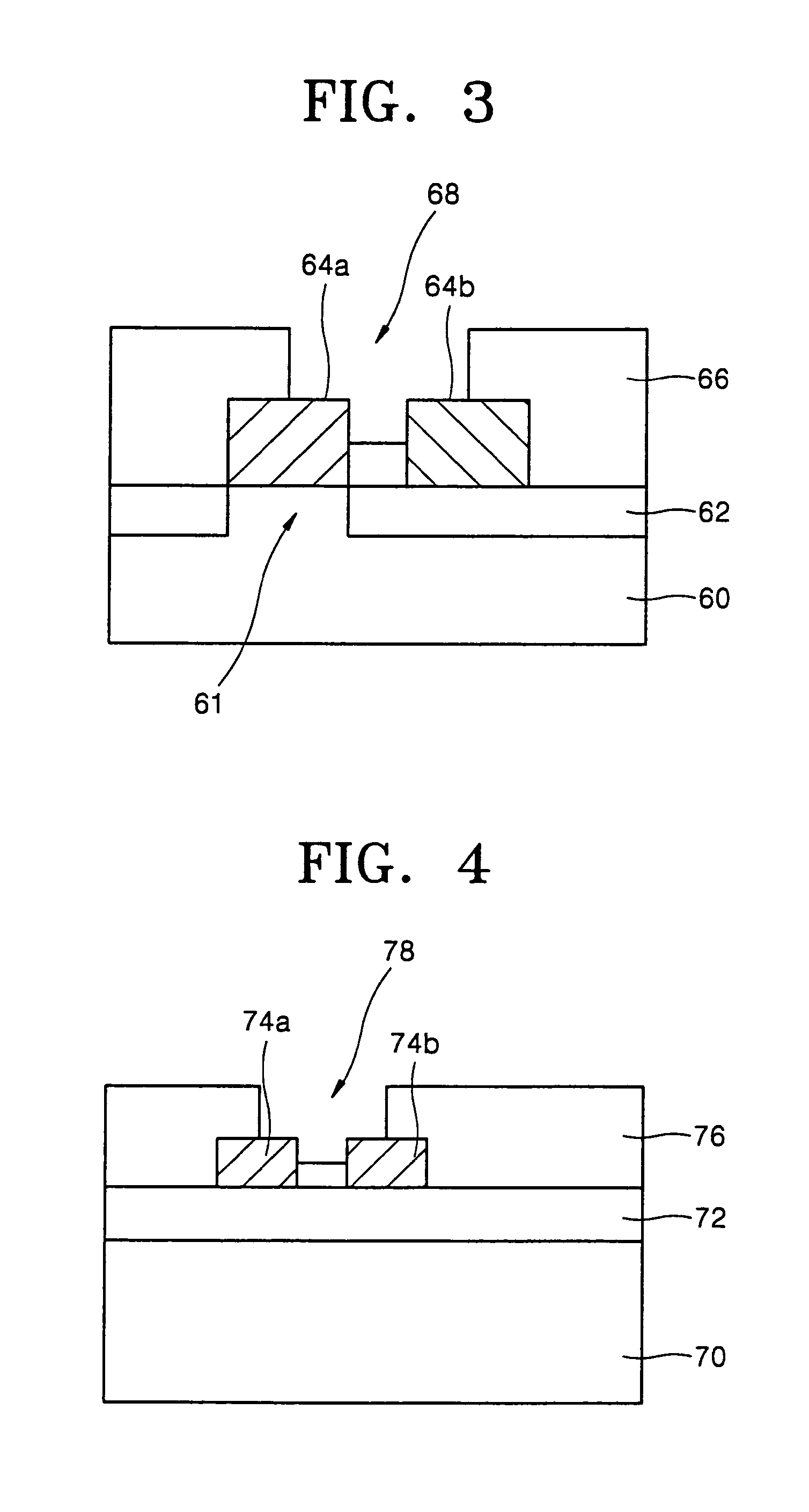
[0016]The following description of an embodiment is provided for a person of ordinary skill in the art to fully understand the present invention. Many changes to the following embodiment are possible, and thus, the present invention is not restricted to this embodiment. The size or thickness of a layer or a film presented in the appended drawings may be somewhat exaggerated for clarity. Also, when a layer is described as being formed on another layer or a semiconductor substrate, the layer may be formed directly on the other layer or semiconductor substrate, or other layers may be interposed therebetween. Like reference numerals in the drawings denote the like members.

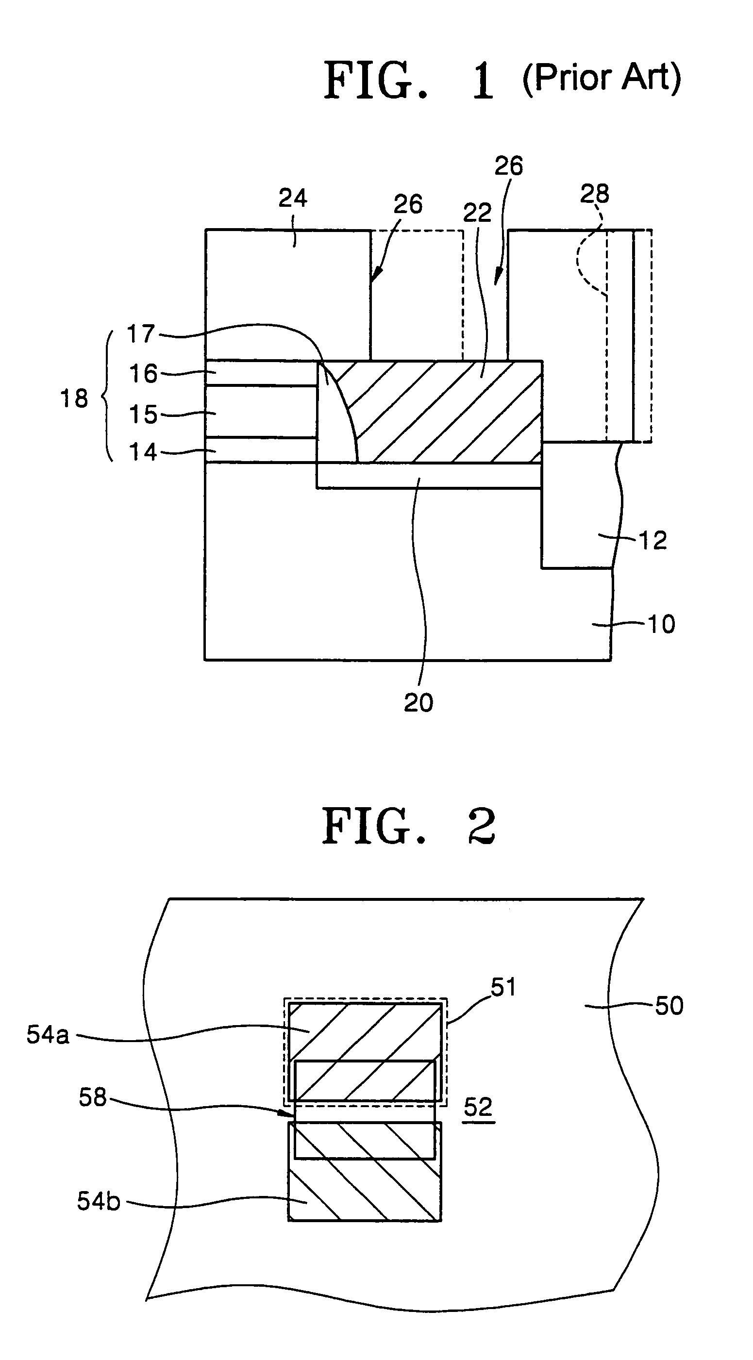
[0017]FIG. 2 is a plan view of a contact structure of an integrated circuit device according to the present invention.

[0018]Referring to FIG. 2, a conductive region 51 and an insulating region 52 are defined on a semiconductor substrate 50. The conductive region 51 can be an active region or metal wiring and the insula...


PUM


Abstract

An integrated circuit device structure which avoids misalignment when a contact hole is formed to expose a contact pad and a method of fabricating the same, are provided. The integrated circuit device includes a semiconductor substrate having a conductive region and an insulating region, a contact pad on the conductive region of the semiconductor substrate, an auxiliary pad adjacent to the contact pad, and an interlevel insulating layer on the semiconductor substrate and having a contact hole for exposing both the contact pad and the auxiliary pad.

Description

RELATED APPLICATION[0001]This application is a divisional of U.S. application Ser. No. 10 / 171,247, filed Jun. 12, 2002, which issued as U.S. Pat. No. 6,699,762 and which claims priority from Korean Patent Application No. 2001-0035110, filed on Jun. 20, 2001, the contents of each of which are herein incorporated by reference in their entirety.FIELD OF THE INVENTION[0002]The present invention relates to integrated circuit devices and a methods of fabricating the same, and more particularly, to integrated circuit device structures and methods for forming contact holes.BACKGROUND OF THE INVENTION[0003]FIG. 1 is a cross-sectional view of a general semiconductor device having a self-alignment contact pad. Referring to FIG. 1, an isolation layer 12, which defines an active region, is formed in a predetermined region on a semiconductor substrate 10 through a general shallow trench isolation (STI) method. Next, a gate electrode 18 is formed on a predetermined portion of the semiconductor sub...

Claims


Application Information

Patent Timeline
Patent Type & Authority Patents(United States)
IPC IPC(8): H01L23/52H01L21/28H01L21/3205H01L21/768H01L23/485
CPCH01L24/02H01L2924/01004H01L2924/01033H01L2924/30105H01L2924/14H01L24/05H10B99/00H01L21/28
Inventor YANG, WON-SUKKIM, KI-NAM
Owner SAMSUNG ELECTRONICS CO LTD
Why Eureka
Try Eureka