

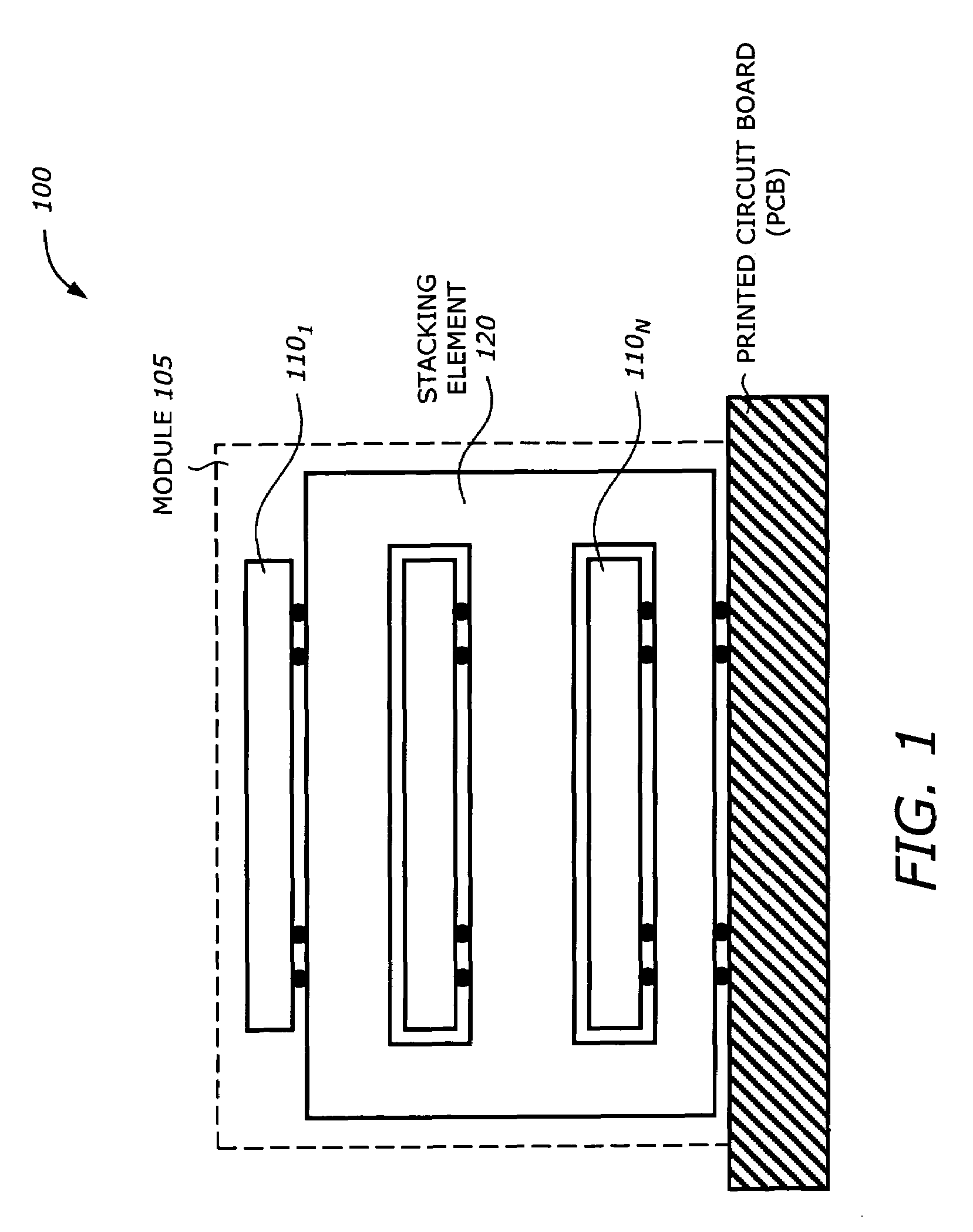
Stacking multiple devices using flexible circuit
a flexible circuit and integrated circuit technology, applied in the field of packaging, can solve the problems of inapplicability of existing techniques to stack multiple devices in other chip packages, many challenges to the board assembly process, and inability to meet the requirements of bga packaging,
- Summary
- Abstract
- Description
- Claims
- Application Information
AI Technical Summary
Problems solved by technology
Method used
Image

Examples
Embodiment Construction
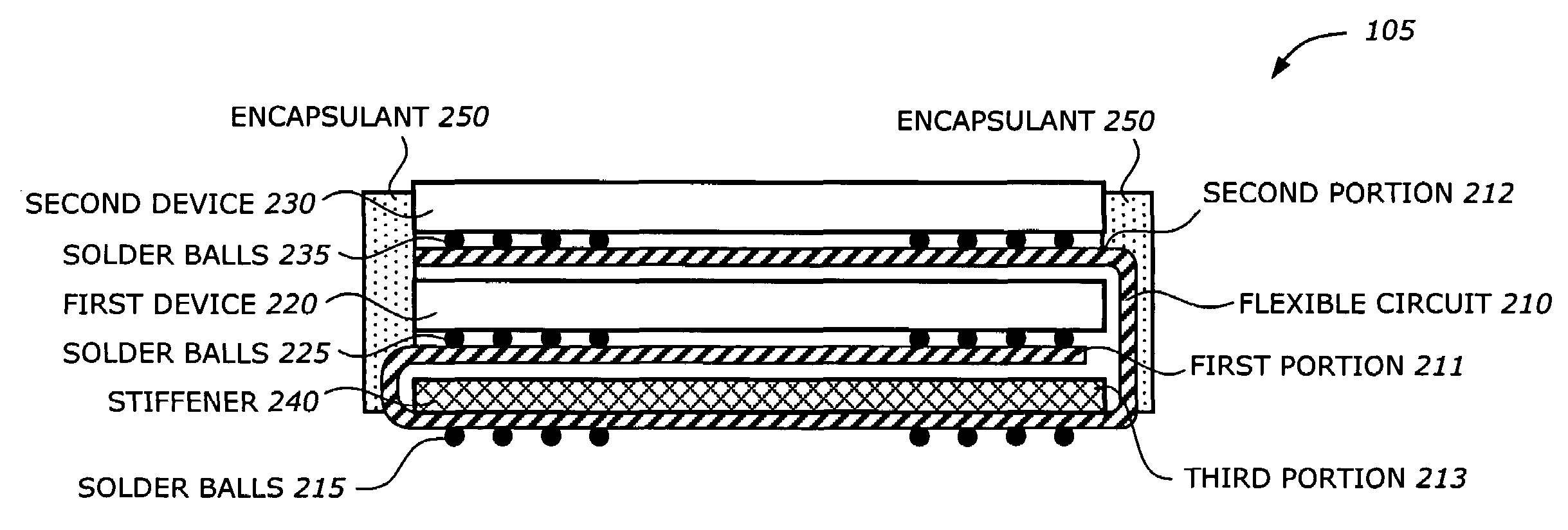
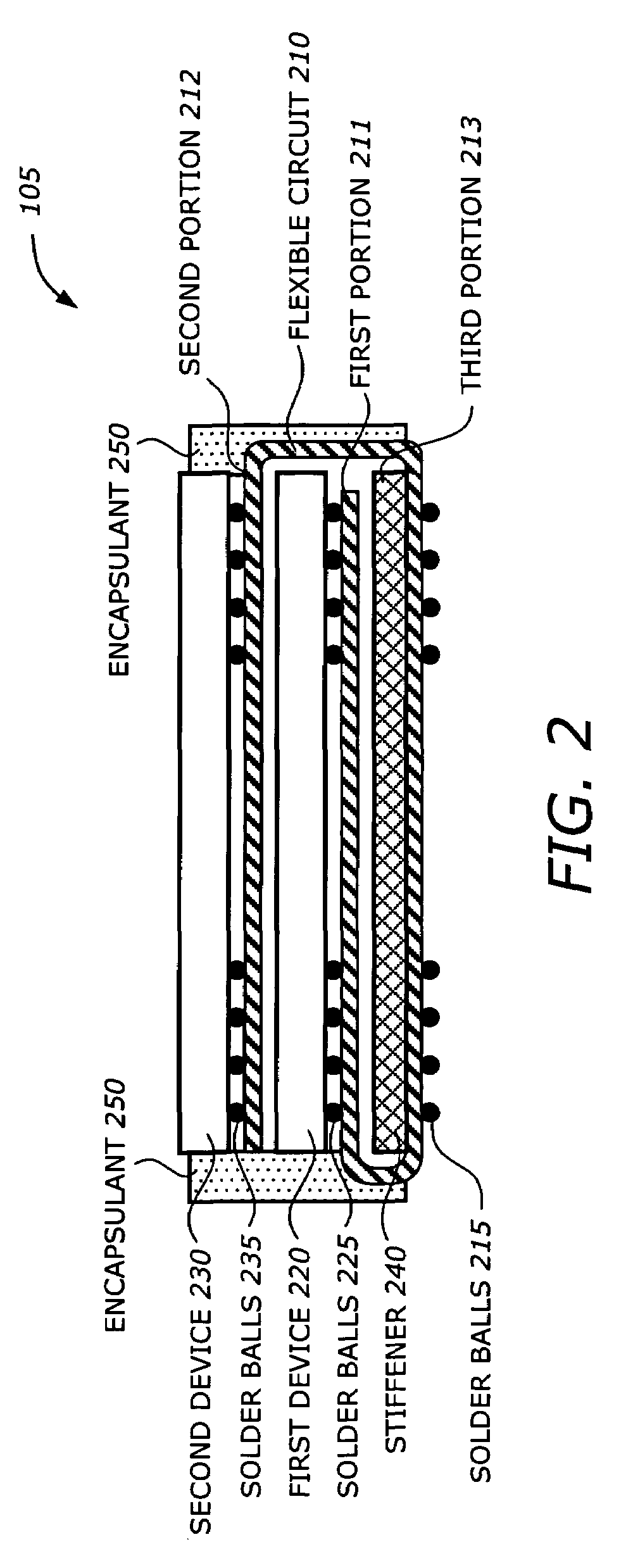
[0014]The present invention is a technique for stacking multiple integrated circuit (IC) devices. One embodiment of the invention includes a flexible circuit and a stiffener. The flexible circuit has first, second, and third portions. The first portion is folded on an upper surface of the third portion and has first contact elements attached to a first device. The second portion is folded on the first device and has second contact elements attached to a second device. The stiffener is attached to the upper surface of the third portion and located between the upper surface of the third portion and the first portion.
[0015]In the following description, for purposes of explanation, numerous details are set forth in order to provide a thorough understanding of the present invention. However, it will be apparent to one skilled in the art that these specific details are not required in order to practice the present invention. In other instances, well-known structures are shown in block dia...
PUM
| Property | Measurement | Unit |
|---|---|---|
| Flexibility | aaaaa | aaaaa |
| aaaaa | aaaaa |
Abstract
Description
Claims
Application Information