Semiconductor device and production method thereof

a technology of semiconductor devices and production methods, applied in semiconductor devices, semiconductor/solid-state device details, electrical apparatus, etc., can solve the problems of unfavorable secondary connection reliability decline, yield decline, and development progress, so as to prevent warps, reduce yield, and reduce secondary connection reliability

Active Publication Date: 2007-01-30
SONY CORP
View PDF7 Cites 8 Cited by
  • Summary
  • Abstract
  • Description
  • Claims
  • Application Information

AI Technical Summary

Benefits of technology

[0014]An object of the present invention is to prevent the arising of warps of a semiconductor wafer when an insulating layer in rewiring layers becomes thick in a SiP type semiconductor device, which may cause an adsorption error and a conveyance error in a production facility, breakage, a decline of the yield and a decline of secondary connection reliability due to residual stress.

Problems solved by technology

Furthermore, development has been advanced to a complicated type of package called a system-in-package (SiP) wherein a passive element, such as a coil, and other semiconductor chips are buried in an interlayer of an insulating layer for insulating rewiring layers formed on a semiconductor substrate (chip) and packaged at a wafer level.
When warps arise on the semiconductor wafer, an adsorbent error and a conveyance error may be caused in a production facility and breakage and a decline of the yield may also be brought.
Furthermore, a disadvantage of a decline of secondary connection reliability is unfavorably caused due to residual stress.

Method used


Image

  • Semiconductor device and production method thereof
  • Semiconductor device and production method thereof
  • Semiconductor device and production method thereof

Examples


example

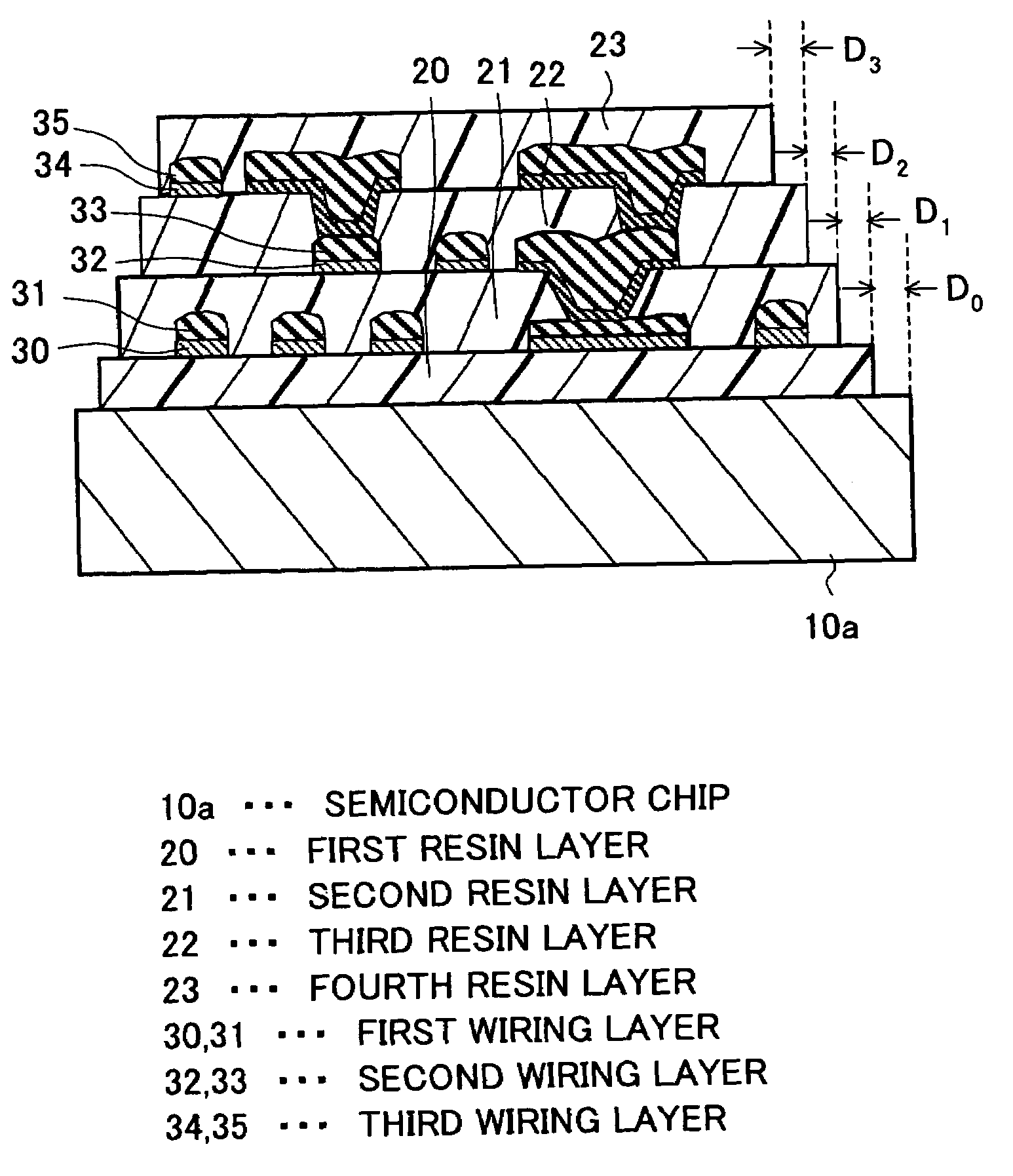
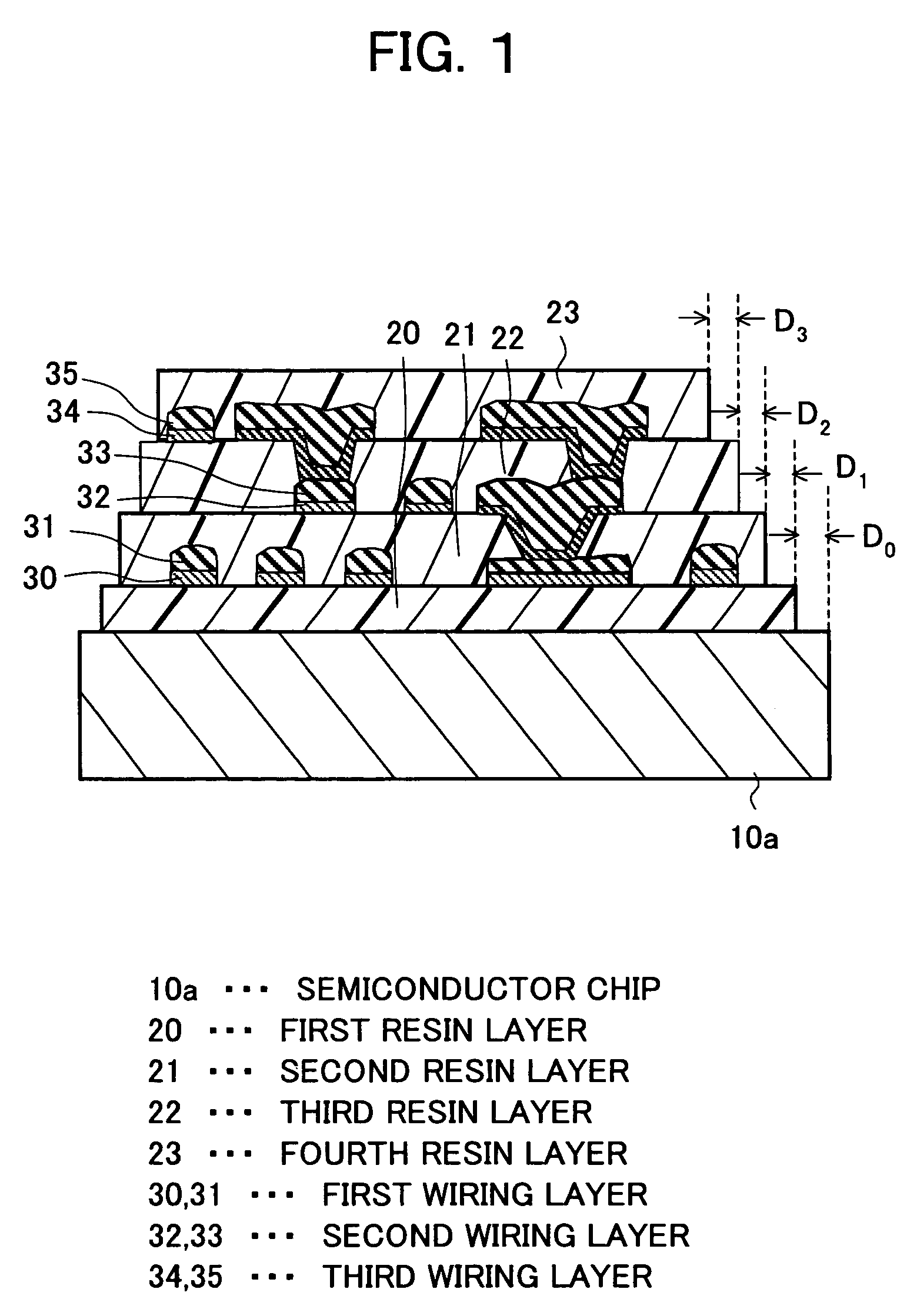
[0066]In the case of forming a resin layer as four stacked layers (a film thickness of 50 μm in total) on a semiconductor wafer, on which semiconductor chips of 3 mm square are integrated, warps of the semiconductor wafer (a distance of one end portion floating from a plane when pressing the other end of the wafer on the plane) could be reduced by 200 μm by applying the present embodiment.

[0067]As explained above, in the production method of a semiconductor device according to the present embodiment, resin layers on the scribe line are removed when stacking the resin layers at a wafer level, and furthermore, a side surface and an upper surface of each of the resin layers are formed to be a stepwise shape, so that warps of the semiconductor wafer can be prevented even without using a resin layer material having special properties.

[0068]Also, since the film thickness of the resin layers stacked on the surface other than the scribe line causes warps, the film thickness of the stacked r...


PUM


Abstract

A semiconductor device and a production method thereof capable of reducing warps of a semiconductor wafer when packaging at a wafer level in a SiP type semiconductor device, is configured that an insulating layer is formed by stacking a plurality of resin layers on a semiconductor chip formed with an electronic circuit, wiring layers are buried in the insulating layer and electrically connected to electrodes, and formation areas of the plurality of resin layers become gradually smaller from an area of an upper surface of the semiconductor chip as they get farther from the semiconductor chip, so that a side surface and an upper surface of each of the resin layers and the upper surface of the semiconductor chip form a stepwise shape.

Description

BACKGROUND OF THE INVENTION[0001]1. Field of the Invention[0002]The present invention relates to a semiconductor device a the production method therefor, and, particularly to a semiconductor device of a type called a system-in-package (SiP), which is packaged at a wafer level, and a production method therefor.[0003]2. Description of the Related Art[0004]Demands for more compact, thinner and lighter portable electronic devices, such as digital video cameras, digital cellular phones, and notebook computers, only get stronger. To respond thereto, seven tenths of a reduction has been realized in three years in a recent VLSI and other semiconductor devices, while studies and developments have been made on the significant issue of how to improve packaging density of components on a mounting board (printed wiring board) in an electronic circuit device wherein such a semiconductor device is mounted on a printed wiring board.[0005]For example, the package type of a semiconductor device has s...

Claims


Application Information

Patent Timeline
Patent Type & Authority Patents(United States)
IPC IPC(8): H01L23/48H01L23/52H01L29/40H01L29/73H01L29/74H01L21/768H01L21/78H01L23/12H01L23/522H01L23/532H01L25/00
CPCH01L21/78H01L23/53238H01L23/53295Y10S257/92H01L2924/0002H01L2924/00
Inventor YAMAGATA, OSAMU
Owner SONY CORP
Why Eureka
Try Eureka