Method for manufacturing printed wiring board

a printing method and wiring board technology, applied in the direction of resistive material coating, solid-state devices, non-metallic protective coating applications, etc., can solve the problems of difficult collectively pressing a plurality of sets of laminated bodies, difficult to reduce the number of laminated bodies that can be received by a pressing machine with a fixed width, and uneven configuration of printed wiring boards. , to achieve the effect of improving thermal circulation, reducing the number of smoothing plates, and increasing the number of lamina

Inactive Publication Date: 2007-02-06
NODA SCREEN
View PDF9 Cites 6 Cited by
  • Summary
  • Abstract
  • Description
  • Claims
  • Application Information

AI Technical Summary

Benefits of technology

[0009]The object of the present invention is not to make a multilayered substrate by forming an insulating layer on circuit patterns as in the conventional case, but to provide a flat substrate with exposed circuit patterns by filling the spaces between the circuit patterns with resin. Accordingly, the adjustment of the thickness of the resin layer on the circuit patterns is not required. The resin only needs to be pressed to the very limit of the height of the circuit patterns so as to leave as little resin as possible on the circuit patterns and to fill the resin into the spaces between the circuit patterns. As a result, a pair of smoothing plates only needs to be arranged on the outermost parts of the plurality of sets of laminated bodies. In this way, by reducing the number of smoothing plates at the time of pressing it is possible to increase the number of laminated bodies received in a pressing machine having a predetermined width. It is also possible to improve the thermal circulation at the time of heating. Consequently, the productivity can be greatly improved. Further, a similar operating effect can also be obtained even when the above described circuit patterns are formed on both sides of a substrate.
[0010]Additionally, a metallic foil with a roughened surface facing the resin may be interposed between the smoothing plate and the resin prior to the time of pressing the smoothing plate against the resin on the substrate. This allows the resin to more easily spread thinly and also causes the surface of the resin to be formed in a fine uneven state corresponding to the roughened surface of the metallic foil. As a result, the residual resin layer can be more easily polished.

Problems solved by technology

As a result, the printed wiring boards are generally formed into an uneven configuration.
In the above described circumstances, the pressing condition may be so demanding that it is difficult to collectively press a plurality of sets of laminated bodies.
However, the above described method of performing collective pressing by arranging smoothing plates between respective laminated bodies has a problem in that the number of laminated bodies that can be received by a pressing machine with a fixed width is reduced by the thickness of the plurality of smoothing plates.

Method used


Image

  • Method for manufacturing printed wiring board
  • Method for manufacturing printed wiring board
  • Method for manufacturing printed wiring board

Examples


Embodiment Construction

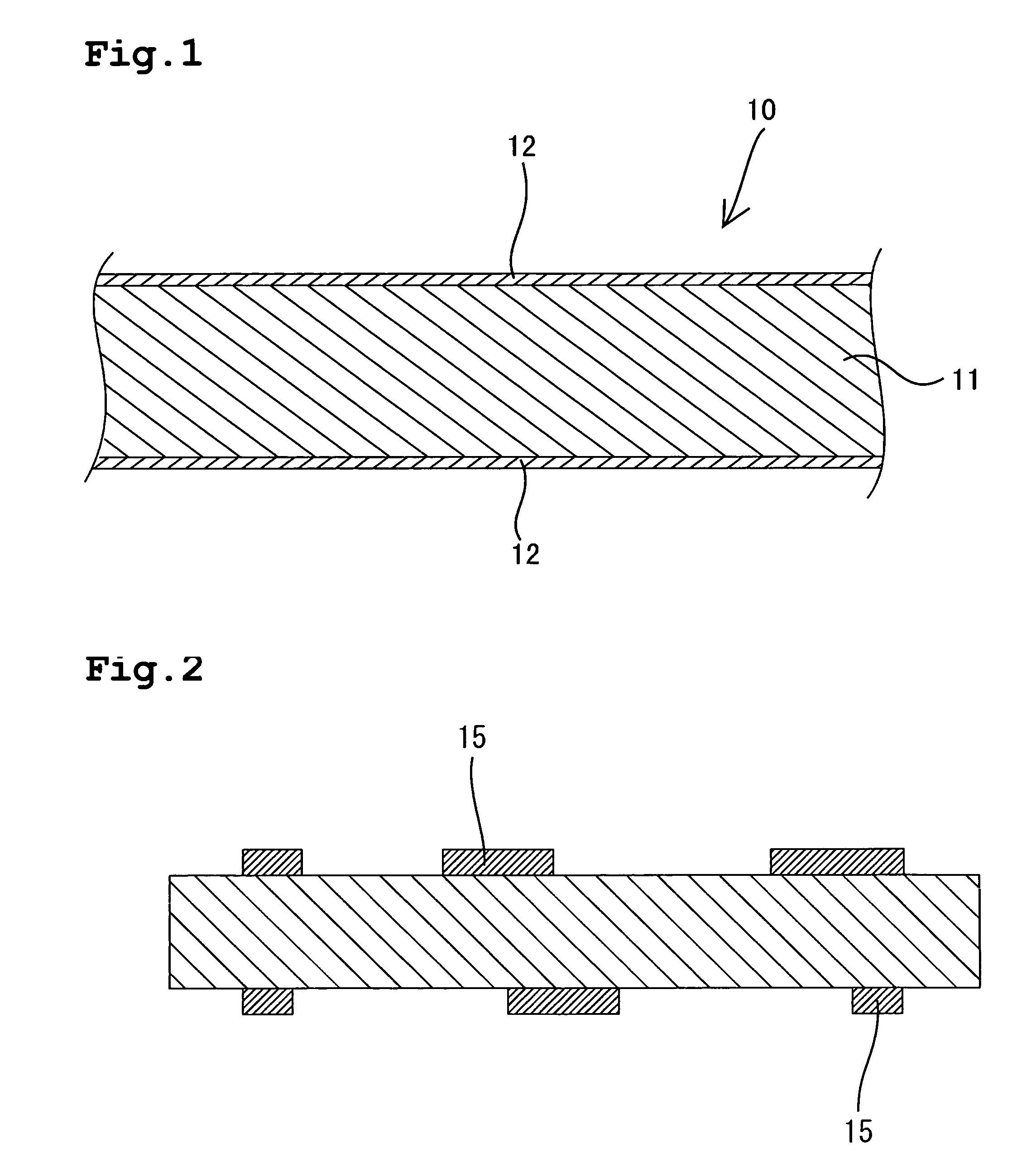
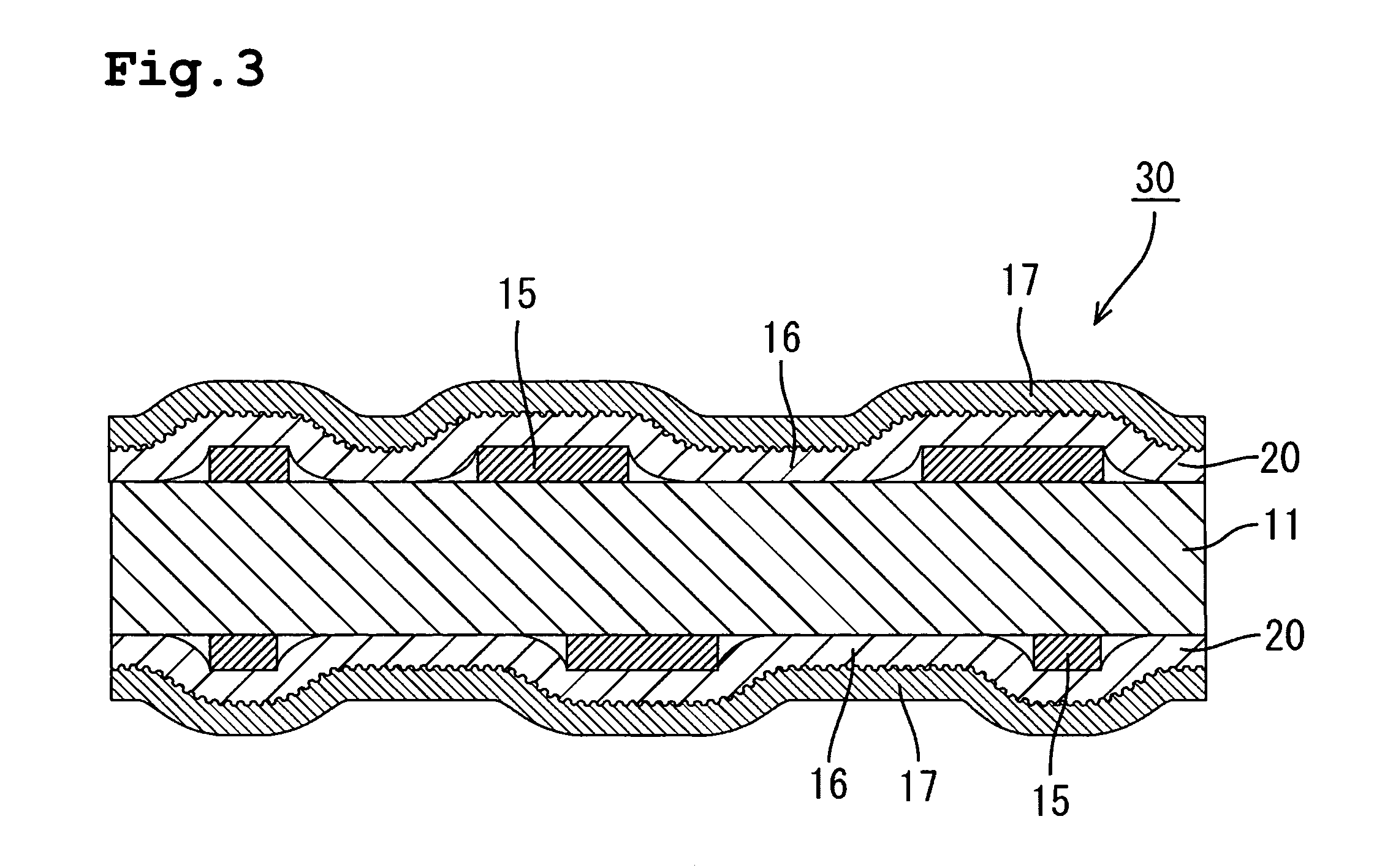
[0019]In the present embodiment, as shown in FIG. 1, a copper clad laminated board 10 is used as a base material in which copper foils 12 are adhered to both sides of a glass epoxy substrate 11 with a thickness of 100 μm to 3000 μm. Circuit patterns 15 are formed on the copper clad laminated board 10 by a known photoetching method (see FIG. 2).

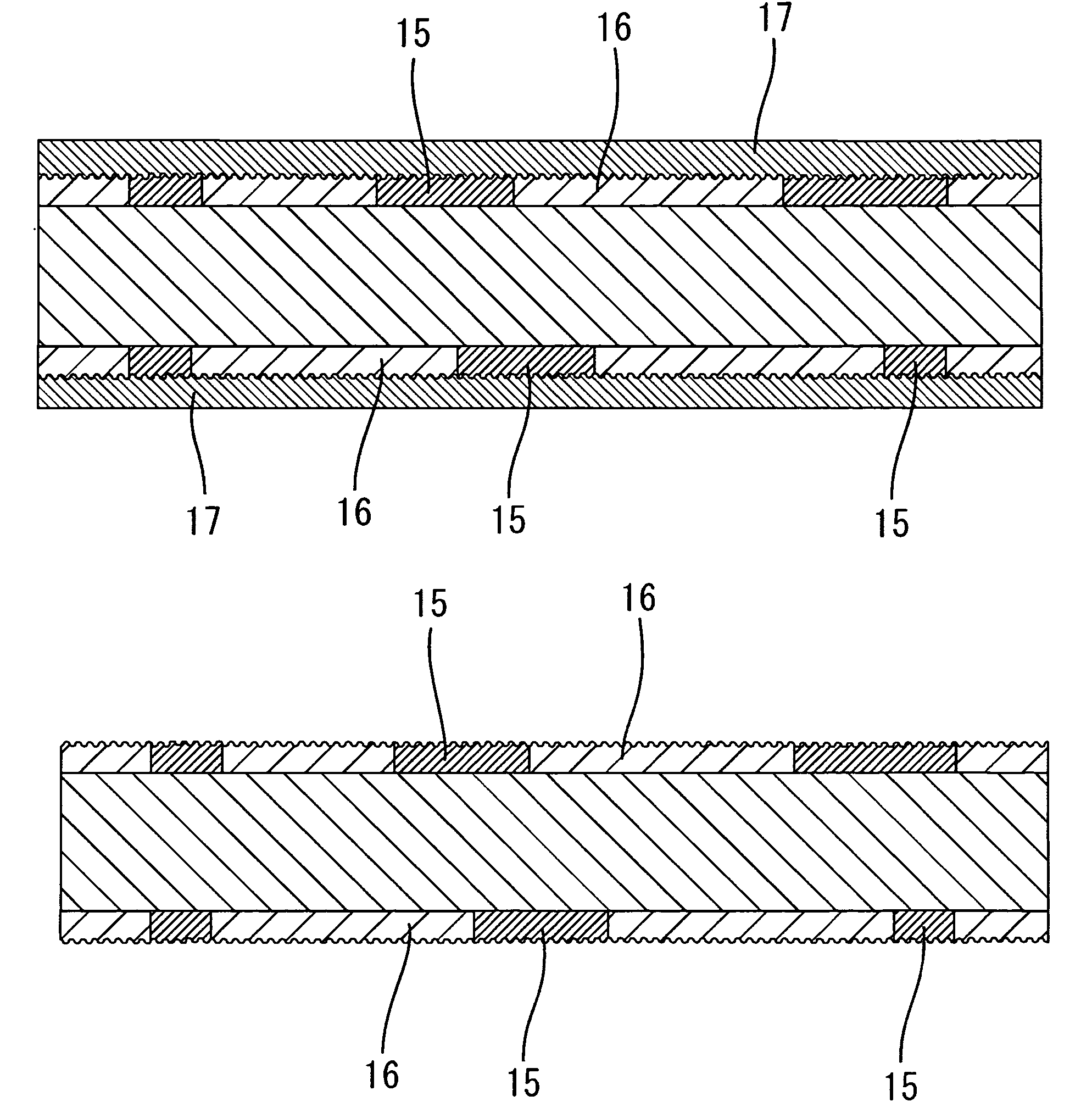
[0020]Next, as shown in FIG. 3, resin layers 16 are formed on the substrate by laminating resin sheets 20 with a thickness of about 30 μm, which are formed by e.g. semi-cured thermosetting epoxy resin, onto the circuit patterns 15 of the wiring board. On the resin sheets 20, nickel foils 17, having a thickness of 18 μm and one face of which is roughened by a needle shaped plating, are also laminated beforehand such that the roughened surface faces the resin sheet 20. At this time, minute air bubbles may also be contained in the resin layer 16. Additionally, the surface of the resin layers 16 is in a gradually rising / falling (i.e., undulating) ...


PUM

PropertyMeasurementUnit
thicknessaaaaaaaaaa
thicknessaaaaaaaaaa
thicknessaaaaaaaaaa

Abstract

There is provided a method for manufacturing a flat printed wiring board in which spaces between circuit patterns are filled with a resin. The method comprises: laminating via a mold release film a plurality of sets of laminated bodies formed by superposing a semi-cured resin sheet on a printed wiring board with circuit patterns formed thereon; placing the laminated plural sets of the laminated bodies interposed between a pair of smoothing plates and collectively pressing the laminated bodies in a reduced pressure atmosphere used for curing the resin; and then polishing the cured resin covering the circuit patterns, thereby exposing the circuit patterns.

Description

TECHNICAL FIELD[0001]The present invention relates to a method for manufacturing a flat printed wiring board in which spaces between circuit patterns are filled with a resin.BACKGROUND ART[0002]In the case of manufacturing a multilayer printed wiring board by e.g. a build-up method, it is necessary to flatten the surface of a lower layer substrate in order to increase the wiring density. However, the circuit patterns of a printed wiring board may be manufactured by a subtractive method for removing unnecessary parts of copper foil via etching. As a result, the printed wiring boards are generally formed into an uneven configuration. The part representing the circuit pattern typically rises above the surrounding surface of the base material.[0003]Therefore, in order to flatten a printed board in which the surface is formed in an uneven form as described above the following method has been proposed. The method comprises laminating a semi-cured resin sheet onto circuit patterns; pressin...

Claims


Application Information

Patent Timeline
Patent Type & Authority Patents(United States)
IPC IPC(8): H01L21/00B05D5/12H05K7/02H05K3/22H05K3/28
CPCH01L21/4857H01L23/49822H05K3/281H05K2201/09881H05K2203/025H05K2203/0278H05K2203/0537H01L2924/0002H05K2203/066H05K2203/085H05K2203/1152H05K2203/1536H01L2924/00
Inventor MURAKAMI, KEIICHI
Owner NODA SCREEN
Why Eureka
Try Eureka